The invention is a novel method for manufacturing porous semiconductors, including silicon (Si), gallium nitride (GaN) and silicon carbide (SiC). The method... The invention is a novel method for manufacturing porous semiconductors, including silicon (Si), gallium nitride (GaN) and silicon carbide (SiC). The method involves applying a thin, discontinuous metallic (preferably platinum) layer to a semiconductor wafer, prior to using common wet chemical etchants (e.g., hydrogen fluoride, hydrogen peroxide), to produce porous silicon (PSi) or other porous semiconductors (PGaN, PSiC). DetailsPorous semiconductors are of interest for their novel optical, electronic, and chemical properties, with PSi being of particular interest. This technology applies a thin, discontinuous layer of metal to a semiconductor wafer before using a wet chemical etching process to produce a controlled thickness of porous semiconductor. The process can be adjusted to produce specific morphologies and desired light emission spectral and/or spatial distributions. How it WorksThis technology introduces a thin, metal catalyst film (a few nanometers in thickness) onto the semiconductor wafer surface, prior to immersion in an aqueous, oxidizing solution of hydrofluoric acid and hydrogen peroxide (i.e., H2O2 metal-HF etching). This process results in the simple and effective production of porous semiconductor. The simplicity and patterning capability will enable large-scale production. PSi with various morphologies, etch depths, and luminescent properties can be produced by adjusting the type(s) of metal layer deposited (gold, platinum, or gold/palladium) as well as the dopant type and level (p+, p-, or n+) of the silicon. Why It Is BetterCurrent methods for generating PSi use anodic etching. In anodic etching, a silicon wafer with attached electrodes and leads is submerged in a wet chemical bath and an electrical bias is applied to drive the etching process. While PSi is not commonly used today in optical or electrical devices, anodic etching is used routinely to generate PSi used to fabricate silicon-on-insulator (SOI) wafers for the electronics industry. A drawback of anodic etching is the extra infrastructure and complexity of applying an electrical bias to a thin wafer submerged in an etchant. At a minimum, it requires electrodes, leads, a power supply, and control electronics. This new technology is an elegantly simple alternative to anodic etching. It is an electroless technique, i.e., external electrical bias is not required, that circumvents all electrical accessories and associated methods. This novel process is also robust, controllable, and even allows flexibility for generating PSi in selected areas rather than across the entire wafer. In addition, this technology provides up to an order of magnitude enhancement in the luminescent properties of PSi compared to those of material produced using anodic etching. Furthermore, researchers may find applications for PSi that would never be possible using anodic etching. ApplicationsPSi could be used in the following emerging applications: - Light-emitting diodes (LEDs)
- Chemical/Biological sensors
- Compliant substrates for heteroepitaxial growth (e.g., nitrides)
- Sacrificial layers for microelectromechanical devices Low-dielectric interconnects
Benefits- Enhanced Control over Product Properties: Both the morphology and light-emitting properties (spatial profile, wavelength) of the semiconductor can be tailored as a function of metal deposited, semiconductor doping level, semi-doping type, and etch time.
- Simple and Robust Process: By using metal deposition and etching, both simple, accepted processes in microelectronics, this "contactless" technology does not require the presence of electrical contacts or other stimuli/equipment to control etching.
- Directed Area Etching/Luminescence: Selective deposition or patterning of the metal catalyst allows controlled creation of etch variations in substrates below and adjacent to the metal. This method can also create selected areas with unique emission properties.
- Promising Potential Properties: This technology might lead to in situ contacts for porous semiconductors/silicon; have potential for ten-fold better luminescent emission from PSi than that obtained from anodic etching; enhance the emission of other semiconductors beyond silicon (e.g., GaN) or enable compliant substrates for heteroepitaxy; and enable creation of PSi on a variety of substrate shapes and sizes.
|
Distributed Bragg Reflectors (DBRs) are a fundamental component of optical devices requiring an optical gain, such as various types of semiconductor lasers.... Distributed Bragg Reflectors (DBRs) are a fundamental component of optical devices requiring an optical gain, such as various types of semiconductor lasers. Conventional methods of forming DBRs require high numbers of layers of semiconductor materials to get the desired reflective resolution. This new method of forming DBRs controls the microstructure of the layers and offers improved vertical cavity surface emitting lasers (VCSELs) and resonant cavity light emitting diodes (LEDs). This technology is a method for making a highly reflective interface for distributed Bragg reflectors (DBRs), which are used in VCSELs and resonant cavity LEDs to generate optical activity. Using Group III-V materials, the interface consists of amorphous layers that contain aluminum, which when oxidized significantly increases the refractive index. As a result, the number of layers needed for the DBR can be reduced from about 30 to 4 or 5. A key element of this technology is that by using a combination of alternating polycrystalline and amorphous materials the layers can be applied to any surface, regardless of the substrate's lattice constant. Therefore, the DBR can be created on any substrate, including glass and silicon, and has a wider range of design possibilities. Additionally, changing the thickness of the layers allows reflectors of different wavelengths to be created. Highly reflective DBRs which reflect in the short wavelength of the visible spectrum and deep into the ultraviolet wavelength can be formed by this method. This technology has been tested extensively with the most common material sets, gallium arsenide (GaAs) and gallium phosphide (GaP) systems. Benefits- Enables fabrication on any surface, even silicon, widening the range of useful materials and designs.
- Decreased processing due to reduced number of layers Increased options for substrate material, including silicon, glass, and other low-cost options.
- Increased design options, particularly when integrating into electronics and optical devices Improved tolerance of temperature variation due to the DBRs more stable characteristics
|
The technology is a chemical method for preparing ultrathin oxide films on silicon with low leakage currents and high capacitance, optimizing the electrical... The technology is a chemical method for preparing ultrathin oxide films on silicon with low leakage currents and high capacitance, optimizing the electrical properties of the dielectric barrier. DetailsAn alternative gate dielectric material will be required for scaling of microelectronic devices to continue at its present rate. The decreasing dimensions of the transistor have required thinner and thinner gate oxide films to maintain capacitance. Unfortunately, leakage currents through silicon dioxide film become too high when using films thinner than 2 nm. Alternative gate oxide materials with a higher dielectric constant have been sought, but the problem has been finding a material which will not form an interfacial layer of silicon dioxide between the high-k dielectric and silicon substrate, and can be deposited using an economically viable process. Continuous dielectric films for silicon based electronics of thicknesses far less than is possible with SiO2have been demonstrated, with high chemical purity and exceedingly low leakage current. This is accomplished through repeated condensation-hydrolysis reactions using n-propyl orthozirconate. The resulting materials will permit the best FET gate material, and when combined with other innovations, the lowest power, highest speed transistors possible. ApplicationsThe primary application for this technology is for integrated circuits; processors and memory applications are the main applications for IC (integrated circuit) technology. Examples of such applications include: - Semiconductors
- Microelectronics fabrication
- Electronic chemical industries
- Tool manufacturing
Other applications would include sealing or passivation of silicon surfaces in electronics and capacitors on chips. Benefits- Smaller, Faster, & More Efficient: High dielectric constant material allows for continuation of size reduction and increased area density
- Increased purity: Key to this technology is the purity of the zirconium Industry potential: High dielectric constant material with low leakage currents
|
Developed by the University of Illinois at Urbana-Champaign, this suite of six technologies enhances multiple facets of nanolithography and scanning probe... Developed by the University of Illinois at Urbana-Champaign, this suite of six technologies enhances multiple facets of nanolithography and scanning probe microscopy. The suite features multifunctional, active probe arrays that enable nanoscale and microscale printing with multiple fluids, nanotube micromachining techniques for high-resolution probe tips, fluid dispensing systems for multiple probes, and a simple electrostatic actuation method for independently lifting individual probes in a high-density probe array. Used singularly or combined, the technologies each offer unique qualities and benefits that simplify and enhance both nanolithography and scanning probe microscopy. ApplicationsThe methods and materials that these technologies utilize can be applied to all types of scanning probe nanolithography as well as scanning probe microscopy. Applications include: - Biotechnology: High-density microarrays or biochips for genomics, toxicology, proteomics, and biological and chemical sensing.
- Semiconductors: Microelectronic components, photomask repair, and direct-write nanolithography.
- Imaging: High throughout scanning probe microscopy, mapping surface characteristics, and detecting surface defects.
BenefitsUsing essentially the same equipment but with varying probes and software, Scanning Probe Microscopy (SPM) with nanoscale probes offers great potential for both nanolithography and imaging. The Nanotip Engineering Suite enhances the functionality of SPM equipment, offering benefits in applications ranging from bioscience to semiconductors. Miniaturization of semiconductor chips could be greatly advanced with the use of scanning probe nanolithography. In genomics and proteomics, biochips containing arrays of dots such as DNA fragments allow researchers to study the vast number of interactions of various proteins on a single chip. Like semiconductor chips, the development of nanoscale scanning probes has great potential benefits for the creation and study of biochips. Current scanning probe nanolithography techniques for creating high-resolution patterning have limitations in both resolution and complexity, and they use inefficient processes. The Nanotip Engineering Suite eliminates many of those limitations and improves the overall process for nanolithography as well as scanning probe microscopy. 1. Multifunctional Probe Array (TF04157)Most current scanning probe lithography methods use a single tip or tip array that must be changed if a second "ink" needs to be applied. This probe change also requires calibration in order to maintain alignment and accuracy. Ths step is both time-consuming and inefficient and also often introduces contamination. To address these issues, this technology provides a multifunctional probe array with active probes that can perform direct chemical patterningand imaging sequentially in a singlerun with accurate registration and no need for changing probes. The technology uses actuators to enable individual control of probes for up and down movement as needed. Patterns using different chemicals and ranging from nano- to microscale can be created and then imaged without risk of cross-contamination and while eliminating the inefficiencies of switching probe tips. Benefits- More versatile: An active multiprobe array enables the use of probe tips of differing sizes for generating patterns of differing sizes. Redundant probe tips can also carry different chemicals simultaneously for multi-ink lithography.
- Faster: This technology enables patterning and imaging sequentially in a single run, eliminating the need to change probes and recalibrate.
- Eliminates cross-contamination: By patterning and imaging with different probes within the same array, this technology eliminates the problem of cross-contamination.
- Accurate: Because the tip-to-tip distance in the array is known, accurate registration between patterns is easily achieved.
- Precision control: An integrated thermal actuator allows control to raise or lower individual probes.
2. Probe Fabrication Method and Microcontact Printing Technique (TF02082)Scanning probe microscopes perform measurements using a probe that has a flexible cantilever beam with a sharp tip attached at the distal end. The fabrication methods for these probes have a number of major drawbacks, including time- sensitive and inefficient processes and difficulty in producing uniform sharpness. Because the cantilevers are made of inorganic thin films, high temperatures and multi-step processes are required to produce them. This new method for probe fabrication and microcontact printing eliminates these problems, while producing either a single probe or an array of probes. It uses an efficient process, lowcost materials, and produces a uniform probe profile. This technology also includes a method for microcontact printing using the fabricated probes described above with integrated elastomeric tips and a commercial scanning probe microscope. This method eliminates the costly and timeconsuming need for a photolithography mask by attaching "inks" to the probe tip and creating patterns with connecting dots. This new technique combines the sub-micrometer accuracy and features of the SPM with the chemical versatility and performance advantages of microcontact printing. Benefits- Lower cost: By utilizing a substrate and sacrificial layer, probes can be fabricated at lower cost than with current fabrication methods. Additionally, the direct microcontact printing technique lowers costs by eliminating the need for a photolithographic mask.
- Improved efficiency: Reusing substrate templates to fabricate additional probes saves time as well as maintains consistent size and sharpness.
- Improved performance: Because the microcontact printing technique combines the features of the SPM with the chemical versatility and performance advantages of microcontact printing, sub-micrometer accuracy is enabled.
3. Machining Nanotube-sized Tips from Multiwalled Nanotubes (TF04162)This technology uses an electron beam machining process to sharpen boron nitride nanotubes into fine-tipped probes for use in atomic force microscopes for molecular and nanostructure imaging and surface manipulation. The nanotube probes are of high strength, high Young's modulus of elasticity, and provide high aspect ratios. Benefits- High strength: Because they are formed from multi-walled nanotubes, the resulting tips are very strong.
- High aspect ratio: The tip's fine point and nanometer-scale size enable high aspect ratios for viewing at the atomic level, providing a significant improvement.
4. Atomic force Microscopy (AFM) Fluid Dispensing System for Probe Arrays (TF02040)To meet the need for an arrayed fluid dispensing system for multiple probes, this technology provides fabrication methods for multiple micro-channels connected to an array of fluid wells. This technology allows side-by-side probes to receive individual inks to create high-density arrays, particularly beneficial for studying biochemical substances such as DNA or proteins. Benefits- Multiple Inks: Current technologies for inking nanolithography probes do not allow the placement of unique inks on each probe tip. Individual tip inking allows for application in high-density DNA and protein arrays.
5. Electrostatic Actuators for Controlling Vertical Movement of Probes(TF03110)Problems with existing electrostatic actuators include complex fabrication methods, low deflection and force generation, large footprints requiring much wafer space and widely spaced probe tips. This design and fabrication method for electrostatic actuators uses the substrate surface as an electrode, simplifying fabrication. It also results in greater deflection and force and a much smaller footprint, enabling ultrahigh density probe arrays with improved performance. Benefits- Simplified fabrication: Because this system includes only one electrode (in the probe), fabrication is greatly simplified.
- Smaller footprint: The electrostatic force and probe stiffness are linear functions of the probe width, making the actuation method highly scalable to very small sizes, potentially enabling ultra-high density probe arrays.
- Better performance: High voltage differences can be applied across the electrodes, resulting in high forces and large deflections.
|
A polymer comprises at least two types of monomer units selected from: (1) diethynyl benzene units, (2) triethynyl benzene units, and (3) ester units. After curing... A polymer comprises at least two types of monomer units selected from: (1) diethynyl benzene units, (2) triethynyl benzene units, and (3) ester units. After curing, the polymer may form a condensed polyaromatic dielectric having a dielectric constant of at most 2.0 at 1 MHz, an elastic modulus of at least 7.7 GPa, and a hardness of at least 2.0 GPa. |
This technology provides a technique for fabricating metallic structures with dimensions considerably smaller than 10 nm and the use of a focused electron beam to... This technology provides a technique for fabricating metallic structures with dimensions considerably smaller than 10 nm and the use of a focused electron beam to locally manipulate nanowires with a resolution of about 3 nm. This is the first technology to use an electron beam and achieve such a high resolution of matter manipulation. Metallic devices hold promise for miniaturization because the electronic wavelength is much smaller in metals than in semiconductors. This technology allows users to fabricate metallic structures with dimensions around 4 nm. The method is based on the application of single linear molecules. This type of metallic decoration results in a very thin metallic wire. Researchers have discovered that in order to produce continuous homogenous wires without breaks, one has to use amorphous metals and alloys which exhibit a high adhesion to the molecule. This technology also allows the use of a focused electron beam to locally modify the shape and the morphology of nanowires with a resolution of about 3 nm. A high energy focused electron beam is used for this purpose. The beam is available in a standard transmission electron microscope. Additionally, this technology can produce a nanograin small enough that its charging energy is less than room temperature thermal fluctuation energy. Therefore, these grains can act as room temperature, single-electron tunneling transistors. Also, pronounced quantum-size effects can occur at low temperatures. This technology could potentially lead to single-electron devices smaller than those attainable through conventional semiconductor technology or even to highly integrated quantum computers. Applications:- Miniaturization
- Quantum computers
- Nanowire crystallization, etching and melting
- Superconducting devices
- Single-electron devices
Benefits:Size - The ability to create metallic structures with such small dimensions can be used to improve numerous applications. |
An innovative, cost-effective method for making and integrating fluidic microchannels. This method for ultra-rapid prototyping of microfluidic systems requiring... An innovative, cost-effective method for making and integrating fluidic microchannels. This method for ultra-rapid prototyping of microfluidic systems requiring fewer than 5 minutes from design to prototype uses liquid phase polymerization as an alternative to etching microchannels in silcone or glass. The method consists of introducing liquid prepolymer into a plastic or glass cartridge, exposing the prepolymer to ultraviolet light through a mask to encourage photopolymerization and define channel geometry, removing the unpolymerized prepolymer, and rinsing the resulting microchannel. ApplicationsThe actuators used in this technology require nothing more than the chemicals surrounding them to monitor the chemistry, mimicking chemical balances as they are maintained in the human body. This new method is ideal for biological and medical applications requiring organic materials, no electronics or batteries, bioresponsiveness, and a single, uniform platform for processing. Potential applications include detection of biological and chemical agents, disease, and contaminants, and in vitro diagnostics and therapy devices. Other promising applications exist in the area of microelectromechanical systems (MEMS). BenefitsThe invention greatly reduces the time and cost associated with the creation of microfluidics systems and requires no experience in microfabrication techniques, no cleanroom facilities, and no expensive equipment. Easy integration enables a manufacturing environment to readily incorporate "add-on" fluidics. This new technology allows ultra rapid prototyping and iterative design, affords immediate production of components, and simplifies complex systems |
The invention is a novel method for manufacturing porous semiconductors, including silicon (Si), gallium nitride (GaN) and silicon carbide (SiC). The method... The invention is a novel method for manufacturing porous semiconductors, including silicon (Si), gallium nitride (GaN) and silicon carbide (SiC). The method involves applying a thin, discontinuous metallic (preferably platinum) layer to a semiconductor wafer, prior to using common wet chemical etchants (e.g., hydrogen fluoride, hydrogen peroxide), to produce porous silicon (PSi) or other porous semiconductors (PGaN, PSiC). Porous semiconductors are of interest for their novel optical, electronic, and chemical properties, with PSi being of particular interest. This technology applies a thin, discontinuous layer of metal to a semiconductor wafer before using a wet chemical etching process to produce a controlled thickness of porous semiconductor. The process can be adjusted to produce specific morphologies and desired light emission spectral and/or spatial distributions. This technology introduces a thin, metal catalyst film (a few nanometers in thickness) onto the semiconductor wafer surface, prior to immersion in an aqueous, oxidizing solution of hydrofluoric acid and hydrogen peroxide (i.e., H2O2 metal-HF etching). This process results in the simple and effective production of porous semiconductor. The simplicity and patterning capability will enable large-scale production. PSi with various morphologies, etch depths, and luminescent properties can be produced by adjusting the type(s) of metal layer deposited (gold, platinum, or gold/palladium) as well as the dopant type and level (p+, p-, or n+) of the silicon. Current methods for generating PSi use anodic etching. In anodic etching, a silicon wafer with attached electrodes and leads is submerged in a wet chemical bath and an electrical bias is applied to drive the etching process. While PSi is not commonly used today in optical or electrical devices, anodic etching is used routinely to generate PSi used to fabricate silicon-on-insulator (SOI) wafers for the electronics industry. A drawback of anodic etching is the extra infrastructure and complexity of applying an electrical bias to a thin wafer submerged in an etchant. At a minimum, it requires electrodes, leads, a power supply, and control electronics. This new technology is an elegantly simple alternative to anodic etching. It is an electroless technique, i.e., external electrical bias is not required, that circumvents all electrical accessories and associated methods. This novel process is also robust, controllable, and even allows flexibility for generating PSi in selected areas rather than across the entire wafer. In addition, this technology provides up to an order of magnitude enhancement in the luminescent properties of PSi compared to those of material produced using anodic etching. Furthermore, researchers may find applications for PSi that would never be possible using anodic etching. Applications:- Light-emitting diodes (LEDs)
- Chemical/Biological sensors
- Compliant substrates for heteroepitaxial growth (e.g., nitrides)
- Sacrificial layers for microelectromechanical devices
- Low-dielectric interconnects
Benefits:- Enhanced Control over Product Properties: Both the morphology and light-emitting properties (spatial profile, wavelength) of the semiconductor can be tailored as a function of metal deposited, semiconductor doping level, semi-doping type, and etch time.
- Simple and Robust Process: By using metal deposition and etching, both simple, accepted processes in microelectronics, this "contactless" technology does not require the presence of electrical contacts or other stimuli/equipment to control etching.
- Directed Area Etching/Luminescence: Selective deposition or patterning of the metal catalyst allows controlled creation of etch variations in substrates below and adjacent to the metal. This method can also create selected areas with unique emission properties.
- Promising Potential Properties: This technology might lead to in situ contacts for porous semiconductors/silicon; have potential for ten-fold better luminescent emission from PSi than that obtained from anodic etching; enhance the emission of other semiconductors beyond silicon (e.g., GaN) or enable compliant substrates for heteroepitaxy; and enable creation of PSi on a variety of substrate shapes and sizes.
|
Ohmic contact degradation and gate-sinking are two major degradation mechanisms that cause semiconductor devices, such as high electron mobility transistors, or... Ohmic contact degradation and gate-sinking are two major degradation mechanisms that cause semiconductor devices, such as high electron mobility transistors, or HEMTs, to fail. In general, the rapid diffusion of contact metals into the indium phosphide substrates has restricted processing temperatures to 300C and reliable operating temperatures have been limited to 200C to 250C. This set of technologies embodies two similar methods for improving reliability and performance of contacts in indium phosphide-based semiconductors. Both alleviate the diffusion of metals into the semiconductor substrate, and the resulting impairment of device performance, by changing the composition of the metal contacts. For the first time, enhancement mode high electron mobility transistors (e-HEMTs) are practical in these material systems. Details By substituting a new metallization scheme in ohmic contacts, and an iridium-based metallization for gate contacts, processing can take place at temperatures greater than 400C, offering a processing temperature window 100C to 150C wider than was available previously. Diffusion of the metal into the substrate is reduced, thereby increasing reliability and operating lifetime. In addition, with the increased Schottky barrier height offered by the use of the new gate metallization, a true reliable indium phosphide enhancement mode HEMT, or e-HEMT, is now possible. An e-HEMT draws no power in its "off" state, a significant benefit in mobile communications applications. Applications- Wireless communications
- Satellite communications
- Defense applications
- High-frequency devices
Benefits- Higher temperature annealing
- Reduced diffusion of contact metal into substrate
- Higher reliability
- Higher temperature operation possible
- Enables true enhancement-mode high electron mobility transistors
|
Amorphous and polycrystalline III-V semiconductor including (Ga,As), (Al,As), (In,As), (Ga,N), and (Ga,P) materials were grown at low temperatures on semiconductor... Amorphous and polycrystalline III-V semiconductor including (Ga,As), (Al,As), (In,As), (Ga,N), and (Ga,P) materials were grown at low temperatures on semiconductor substrates. After growth, different substrates containing the low temperature grown material were pressed together in a pressure jig before being annealed. The annealing temperatures ranged from about 300.degree. C. to 800.degree. C. for annealing times between 30 minutes and 10 hours, depending on the bonding materials. The structures remained pressed together throughout the course of the annealing. Strong bonds were obtained for bonding layers between different substrates that were as thin as 3 nm and as thick as 600 nm. The bonds were ohmic with a relatively small resistance, optically transparent, and independent of the orientation of the underlying structures. |
In one embodiment of the present invention an oxygen iodine laser includes a gas mixing section. Ground state oxygen and a carrier gas are introduced into the... In one embodiment of the present invention an oxygen iodine laser includes a gas mixing section. Ground state oxygen and a carrier gas are introduced into the first gas mixing section, sometimes separately. The laser includes a discharge region to generate at least said excited oxygen from the flow of the first gas mixing section. A sensitizer gas having a lower ionization threshold than ground state oxygen is also introduced into the first gas mixing section, such that electrons are more easily produced in the electrical generator. The laser system includes introducing a source of iodine into the excited singlet delta oxygen flow to generate a laser-active gas. In another embodiment a conditioner is placed into the gas mixing section to help mix the flow and/or introduce one or more of the aforementioned gases. |
Electrohydrodynamic jet printing has been largely ignored in the high resolution graphics and electronics fabrication industries because previous methods used... Electrohydrodynamic jet printing has been largely ignored in the high resolution graphics and electronics fabrication industries because previous methods used broad and blunt nozzles that did not provide the resolutions and accuracy of other methods. Because e-jet printing also required a high voltage and led to significant positioning errors, it was restricted to use in modest resolution applications. This new approach to e-jet printing produces a higher resolution using nozzles with much smaller internal diameters than previous methods. In former methods, e-jet printing was limited to dot diameters of ~15 micrometers. This new method can produce dots as small as 250 nanometers and line widths as narrow as 700 nanometers. DetailsE-jet printing uses electric fields to create the necessary fluid flows to deliver inks to a substrate. While this approach has been explored for modest resolutions, this new approach deals specifically with high resolution printing. The e-jet uses nozzles have much smaller internal diameters than previous methods. A voltage applied between the nozzle and the metal plate allows for greater accuracy in high resolution printing. This method is now in development with multiple nozzles which will allow for greatly increased printing speed. Applications- Inkjet and printed electronics industries, as well as the security, biotechnology and photonics industries.
Benefits- Small nozzle internal diameters, less than 30 micrometers, coupled with low volt electric charge, allows for very high resolution printing.
- Can print nearly any chemical composition of ink without requiring a specific type of ink for high resolution printing.
- Distribution of electric field lines through low voltage results in minimal lateral variations and greater accuracy in high resolution printing.
- Can be used to print bulk single walled carbon nanotubes, on almost any substrate.
|
The ability to print a polarized electrical charge onto a medium, or charge patterning, is currently in the early stages of development. A similar technology... The ability to print a polarized electrical charge onto a medium, or charge patterning, is currently in the early stages of development. A similar technology commonly used in office printers, Xerography, thrives in large size regimes. There exist only a few competitive technologies capable of printing at the nanometer scale. Current technologies use processes that provide only low resolutions and relatively poor control over the printed charges. For example, current atomic force microscopy probes can provide suitable charges, but are only able for use on specialized materials. This technology has been designed to enable the printing of electrical charges on a nanoscale resolution. This technology works by modifying an E-Jet printer so that electric charges are used to manipulate a fluid medium and imprint a net positive or negative charge onto a nearly any surface. ApplicationsThis technology may be used for: - Electrostatic control of nano-electric mechanical devices
- Guided assembly of charged particles or nanostructures
- Modulation of activity in biological systems
- Invisible, printed security codes
Benefits- Enables complex patterns of alternating charge with nanoscale resolutions
- Allows highly controlled amounts of material transfer
- Printing can be performed on nearly any surface
|
Researchers from the University of Illinois have developed a process that is fully compatible with conventional foundry processes for manufacturing transient electronics.... Researchers from the University of Illinois have developed a process that is fully compatible with conventional foundry processes for manufacturing transient electronics. Utilizing conventional foundry processes allows high volume, low cost production of transient electronics which may expedite commercialization of transient technology. This technology was developed in the laboratory of Dr. John Rogers, who has received international recognition for his work on bio-integrated electronics. |
Researchers fromt the University of Illinois have developed a method of identifying and removing the metallic carbon nanotubes in an array without damaging the... Researchers fromt the University of Illinois have developed a method of identifying and removing the metallic carbon nanotubes in an array without damaging the semiconducting carbon nanotubes. The method is nearly 100% effective and scalable to large arrays. This technology enables the large-scale creation of CNT arrays with a very high I on/I off ratios. A larger ratio means less lost power while off, faster switching time, and lower operating voltage. This technology was developed in the laboratory of Dr. John Rogers, who has received international recognition for his work on bio-integrated electronics. |
Manufacturers can not achieve superconformal (bottom-up) filling of high aspect ratio features by a modified chemical vapor deposition method. The CVD precursor... Manufacturers can not achieve superconformal (bottom-up) filling of high aspect ratio features by a modified chemical vapor deposition method. The CVD precursor flux is augmented by a small flux of a growth suppressor, which slows deposition near the upper surface of the substrate while permitting growth at normal rates deep in a trench or via. DetailsAs circuit densities increase, the width of their gap structures decrease, making uniform deposition of semiconductor materials more difficult and more expensive. In order to keep-up with the demand for increasing miniaturization, transistor manufacturers have developed several novel alternatives to physical layer deposition. Among the most successful of these alternatives is Atomic Layer Deposition (ALD), a technique that essentially builds thin-film depositions one atom-layer at a time. Atomic layer deposition, however, is slow and must be repeatedly exposed to alternating reactive gasses. Electrochemical Deposition (ECD) has also been used as a solution in increasing circuit densities, but ECD is limited to certain materials and requires an additional "wet processing" step. Superconformal CVD avoids these obstacles through super heating elemental hydrogen or nitrogen, changing the gas into its atomic, or plasmatic, state. During the chemical deposition process, a plasma beam that is directed at the substrate suppresses the chemical reaction along the surface of the etched wafer, preventing undesirable material accumulation around the cusp of the wafer's trenches. ApplicationsFor use in the development of micro- and nano-scale semiconductor devices, Superconformal CVD gives producers of microchips, MEMS, and various other microelectronic devices greater control over their manufacturing process. All current methods of CVD: Superconformal CVD has been demonstrated to be successful for the deposition of several different types of materials. The technique should be widely applicable for the superconformal deposition of essentially any material, although additional development work may be required to identify the best combination of suppressor gas and growth gas. BenefitsThe semiconductor device industry strives to develop manufacturing techniques to meet increasingly stringent design rules. By offering a gas-phase method for achieving superconformal, bottom-up filling of features with high aspect-ratios, this technology solves a long-standing manufacturing obstacle. - Eliminates Pinch-off: Pinch-off occurs when unwanted film deposition near the opening of a trench or via accumulates to the point that the gap closes. Pinch-off creates voids within a trench or via, resulting in reduced device performance. These problems have proven difficult to overcome; alternative manufacturing methods - atomic layer deposition (ALD) and electrochemical deposition (ECD) - require several extra steps.
- Fast and inexpensive: Our Superconformal Chemical Vapor Deposition method is fast and inexpensive and does not require extra chemical washing or polishing steps. The process is compatible with existing microelectronic manufacturing methods.
- Clean deposition: Atomic hydrogen often serves as an effective suppressor gas, and a significant advantage of its use is that impurities are not introduced that could compromise device performance. The metastable nature of the atomic hydrogen ensures that it rapidly recombines on and desorbs from the surface as molecular hydrogen gas.
- High Aspect Ratio Processes: With our improved method, pinch-off is reduced or eliminated, often achieving complete filling even for aspect ratios as high as 50:1.
|
This technology is a family of metal complexes that can be used for depositing metal compounds. This technology is a family of metal complexes that can be used for depositing metal compounds. |
Dr. Bahl from the University of Illinois has discovered a new method to create non-reciprocal property without using external magnetic field. The method employs... Dr. Bahl from the University of Illinois has discovered a new method to create non-reciprocal property without using external magnetic field. The method employs Brillouin Stimulated Induced Transparency (BSIT), by adding a laser and a specifically designed microns-sized resonator. Applying BSIT can significantly reduce the size and cost, and also bring about the possibility for magnet-free on-chip application. |
Dr. Bailey from the University of IL has invented a new fluidic device for droplet manipulation for use in droplet-based analysis, such as PCR in DNA sequencing.... Dr. Bailey from the University of IL has invented a new fluidic device for droplet manipulation for use in droplet-based analysis, such as PCR in DNA sequencing. Sample preparation has been longing an high through-put, automated solution due to its intensive labor cost. This chip-scale fluidic device enables multiple droplet manipulations, such as splitting, addition, extraction in one single geometry. With further development it even has possibility to change droplet concentration. |
The invention improves the process of ion implantation and annealing, which is used to introduce dopants into a semiconductor to make pn junctions. The... The invention improves the process of ion implantation and annealing, which is used to introduce dopants into a semiconductor to make pn junctions. The improvements control the motion of bulk semiconductor defects such as interstitial atoms through control of surface chemistry. This leads to a reduction of the depth and electrical resistance of the pn junction. DetailsThe invention concerns process improvements to ion implantation and annealing technology, which is used to introduce dopants into a semiconductor in order to make pn junctions. The improvements control the motion of bulk semiconductor defects such as interstitial atoms through control of surface chemistry. The surface chemistry changes the intrinsic ability of the surface to absorb defects that diffuse to it. The preferential loss of Si interstitials keeps electrically active dopant fixed in the lattice by inhibiting the "kick out" reaction that makes such dopant atoms mobile and inactive. The interstitial loss rate is controlled by the introduction of an additional step in the annealing process. The surface chemistry also changes the interaction of electrically charged defects with charges at the surface by greatly reducing the charge buildup at the surface and therefore reducing the surface repulsion effect, which increases the activated dopant concentration. ApplicationsThis technology can be applied to almost any product that uses higher end (< 90 nm) integrated circuits. Not relevant to technologies that use lower resolution since current pn junction technology is acceptable. Examples of such applications include: - Computers
- Communications
- Electronics
Benefits- Pn junction with reduced depth and increased dopant activation: Leads to transistor devices with higher performance
- Compatible with current manufacturing technologies: Avoids the large costs associated with paradigm-changing technologies
- Adjusted loss rate of interstitials to the surface: Offers highly controllable mechanism for defect engineering.
|
The invention provides a quantum well active region for an optoelectronic device. The quantum well active region includes barrier layers of high bandgap material.... The invention provides a quantum well active region for an optoelectronic device. The quantum well active region includes barrier layers of high bandgap material. A quantum well of low bandgap material is between the barrier layers. Three-dimensional high bandgap barriers are in the quantum well. A preferred semiconductor laser of the invention includes a quantum well active region of the invention. Cladding layers are around the quantum well active region, as well as a waveguide structure. |
A semiconductor laser that includes an active region, claddings and electrical contacts to stimulate emissions from the active region, where a coupled waveguide... A semiconductor laser that includes an active region, claddings and electrical contacts to stimulate emissions from the active region, where a coupled waveguide guides emission. The waveguide includes a broad area straight coupling region that fans out into an array of narrower Individual curved coupled waveguides at an output facet of the laser. The individual curved coupled waveguides are curved according to Lorentzian functions that define the waveguide curvature as a function of position along the device. The integral length of each individual curved coupled waveguide differs from adjacent individual curved coupled waveguides by an odd number of half-wavelengths. The coupled waveguide array shapes the optical field output of the semiconductor laser such that a large fraction of the power is emitted into a small angular distribution using interference phenomena. A laser of the invention produces high power output with a very high quality, narrow beam shape. |
A method for producing light emission, including the following steps: providing a transistor structure that includes a semiconductor base region disposed between a... A method for producing light emission, including the following steps: providing a transistor structure that includes a semiconductor base region disposed between a semiconductor emitter region and a semiconductor collector region; providing a cascade region between the base region and the collector region, the cascade region having a plurality of sequences of quantum size regions, the quantum size regions of the sequences varying, in the direction toward the collector region, from a relatively higher energy state to a relatively lower energy state; providing emitter, base and collector electrodes respectively coupled with the emitter, base, and collector regions; and applying electrical signals with respect to the emitter, base, and collector electrodes to cause and control light emission from the cascade region. |
Researchers from the University of Illinois have developed a method for vertical-cavity surface-emitting laser (VCSEL) to provide high-power output with good beam... Researchers from the University of Illinois have developed a method for vertical-cavity surface-emitting laser (VCSEL) to provide high-power output with good beam quality. The method use Zn-diffusion to create disordering and filter out high order mode of the laser. As a result, VCSEL with larger aperture, which permits higher power, will still output single mode light with tight focus. This technology provides laser for energy-assisted magnetic recording, which could be used in next generation hard disk drive. |
This invention allows for the production of a family of photodetectors that are sensitive in the ultraviolet, visible, and near-infrared regions of the spectrum.... This invention allows for the production of a family of photodetectors that are sensitive in the ultraviolet, visible, and near-infrared regions of the spectrum. Despite previous knowledge of photo responses to low pressure gas discharges, this technology is the first to achieve these responses without using plasma as the photosensitive element. The plasma instead amplifies the number of photoelectrons produced by the cathode's avalanche effect. Furthermore, the electronic properties of the photocathode material determine the spectral response of the photodetector. These photocathodes can then be composed of different materials to optimize the photodetector for more specific responsiveness. DetailsAs the spatial dimensions of microplasma devices have continued to decrease they have become attractive for an increasingly wide range of applications. The microdischarge devices this technology enables are sensitive detectors of visible, near-IR, and UV radiation and significantly extend the use of silicon devices. The wavelength range over which microdischarge detectors are photosensitive can be extended by simply changing the photocathode material Therefore, detectors have a significant advantage over their semiconductor counterparts because of the wavelength agility available with a single, rugged device structure. Furthermore, the crystalline quality of the semiconductor photocathode in the microplasma device is unlikely to be critical. Consequently, one has the option of micromachining the detector from silicon and overcoating the cathode with a film of the appropriate semiconductor (or other material). Since this detector is fabricated in silicon, large arrays of devices can be produced economically. To date, arrays as large as 250,000 (500 x 500) have been tested successfully. These photodetectors combined with other advances in microdischarge technology lead to a bright future for nearly any application involving light. Information about other devices and applications using UIUC Microdischarge technology is available on request. Benefits- Amenable to mass production: This invention can be readily integrated with other electronic or optoelectronic devices.
- Inexpensive: Because this device does not depend on the existence of a p-n junction the crystalline quality of the semiconductor is not an issue.
- More sensitive: This invention provides a photodetector in the visible and UV that is considerably more sensitive than commercial Si photodiodes.
|
The invention provides in one of the embodiments for either a continuous wave (cw) or pulsed alkali laser having an optical cavity resonant at a wavelength defined... The invention provides in one of the embodiments for either a continuous wave (cw) or pulsed alkali laser having an optical cavity resonant at a wavelength defined by an atomic transition, a van der Waals complex within the optical cavity, the van der Waals complex is formed from an alkali vapor joined with a polarizable gas, and a pump laser for optically pumping the van der Waals complex outside of the Lorentzian spectral wings wherein the van der Waals complex is excited to form an exciplex that dissociates forming an excited alkali vapor, generating laser emission output at the wavelength of the lasing transition. |
Plasma-based electronic devices assumed a significant role in communications and display systems in the first half of the 20th century. One example is the plasma... Plasma-based electronic devices assumed a significant role in communications and display systems in the first half of the 20th century. One example is the plasma voltage regulator (such as the OA, OB, OC, and OD series of rare gas plasma voltage regulators and electronic switches, and the 866A mercury plasma high voltage tube) that was widely incorporated into RF transmitters. This invention demonstrates that portions of a semiconductor transistor can be replaced by plasma, yielding a new family of three terminals, hybrid plasma electronic devices having properties previously unavailable. DetailsThis invention provides hybrid semiconductor-plasma transistors in which the plasma replaces at least one semiconductor portion of a conventional transistor. Preferred embodiments of the invention provide a plasma bipolar junction transistor (PBJT) in which a plasma serves as the collector for an npn BJT. As the plasma conducts current, light is emitted that can be modulated by imposing a time-varying voltage across (or current through) the emitter-base junction of the PBJT. In this and other devices of the invention, the plasma may either be micro-cavity plasma, offering reduced volume and enhanced electron densities relative to macro-scopic plasma, or a larger volume (conventional) low temperature plasma. Other preferred embodiments of the invention provide plasma MOSFET devices in which plasma controls the conductance of the channel in a MOSFET. Applications- Ultra High Resolution
- Plasma Displays
- Next Generation
- Flexible Displays
- Biomedical and Environmental Sensors
- Micro-analytical Instruments having low power consumption
- 3D chips Other applications where traditional transistors are used
BenefitsThese transistors have reduced volumes and are thinner thus the devices formed with these transistors will be smaller and can be used in newer potential applications. The plasma transistors have enhanced electron densities and the plasma modulation can be controlled with very low voltages for the first time and thus the devices will be faster and very energy efficient. |
Researchers at the University of Illinois have developed a new laser pumping method which provides efficient and continuous high power (>10W) lasers in the... Researchers at the University of Illinois have developed a new laser pumping method which provides efficient and continuous high power (>10W) lasers in the visible, ultraviolet, and near-infrared regions in both gas and solid state systems. This method allows cooling of the laser medium while achieving over 100% quantum efficiency. Combined with frequency doubling this laser should yield more than 10 watts of violet (426 or 427 nm), a region of the spectrum in which no powerful sources exist. |
Electrochemical fabrication platforms for making structures, arrays of structures and functional devices having selected nanosized and/or microsized physical... Electrochemical fabrication platforms for making structures, arrays of structures and functional devices having selected nanosized and/or microsized physical dimensions, shapes and spatial orientations. Methods, systems and system components use an electrochemical stamping tool such as solid state polymeric electrolytes for generating patterns of relief and/or recessed features exhibiting excellent reproducibility, pattern fidelity and resolution on surfaces of solid state ionic conductors and in metal. Electrochemical stamping tools are capable high throughput patterning of large substrate areas, are compatible with commercially attractive manufacturing pathways to access a range of functional systems and devices including nano- and micro-electromechanical systems, sensors, energy storage devices, metal masks for printing, interconnects, and integrated electronic circuits. |
This invention is the world's first light emitting transistor. The HBLET extends the capabilities of light-emitting diodes and could make this transistor the... This invention is the world's first light emitting transistor. The HBLET extends the capabilities of light-emitting diodes and could make this transistor the fundamental element in electronics and optoelectronics. DetailsIn a bipolar device there are two kinds of injected carriers, negatively charged electrons and positively charged holes. Some of these carriers, for example, a transistor, recombine rapidly, supported by a base current essential for normal transistor function. In the past, this base current has been regarded as a waste current that generates unwanted heat. However, this technology shows the base current creates light that can be modulated at transistor speed. This recombination process is the same (but enhanced by carrier transport) as the one used in LEDs to produce visible, rather than infared, light. The transistor laser produces infared radiation in phase with its base current, so it can be modulated at a switching speed impossible to attain with an LED. The switching speed obtained is fast enought to operate in fiber optic networks, as well as other applications. These transistors are made with indium gallium phosphide and gallium arsenide, unlike traditional transistors which have been built from silicon and germanium. The recombination process in indium gallium phosphide and gallium arsenide materials create infared photons, the "light" in the light emitting transistor. This contributes to the device's ability to operate as both a laser and a transistor. The existence of a third port (the photon output) can interconnect optical and electric signals for display or communication purposes. Additionally, electrical and optical qualities are increased by the incorporation of quantum wells into the active region of the transistors. The transistor laser has a unique capability in signal processing and electronic-photonic integrated circuits. Applications- Electronics
- Optoelectronics
- Displays
Benefits- Speed: These transistors produce infared light in phase with their base current, allowing it to attain a switching speed superior to light emitting diodes (LEDs).
- Controlled light emission: Light intensity can be controlled by varying the base current.
- Simultaneous control of optical and electrical outputs: The addition of a third port allows greater control.
- Utilizes base current: Once considered wasteful, the base current is used to create light.
|
This invention is the world's first light emitting transistor. The HBLET extends the capabilities of light-emitting diodes and could make this transistor the... This invention is the world's first light emitting transistor. The HBLET extends the capabilities of light-emitting diodes and could make this transistor the fundamental element in electronics and optoelectronics. Details In a bipolar device there are two kinds of injected carriers, negatively charged electrons and positively charged holes. Some of these carriers, for example, a transistor, recombine rapidly, supported by a base current essential for normal transistor function. In the past, this base current has been regarded as a waste current that generates unwanted heat. However, this technology shows the base current creates light that can be modulated at transistor speed. This recombination process is the same (but enhanced by carrier transport) as the one used in LEDs to produce visible, rather than infared, light. The transistor laser produces infared radiation in phase with its base current, so it can be modulated at a switching speed impossible to attain with an LED. The switching speed obtained is fast enought to operate in fiber optic networks, as well as other applications. These transistors are made with indium gallium phosphide and gallium arsenide, unlike traditional transistors which have been built from silicon and germanium. The recombination process in indium gallium phosphide and gallium arsenide materials create infared photons, the "light" in the light emitting transistor. This contributes to the device's ability to operate as both a laser and a transistor. The existence of a third port (the photon output) can interconnect optical and electric signals for display or communication purposes. Additionally, electrical and optical qualities are increased by the incorporation of quantum wells into the active region of the transistors. The transistor laser has a unique capability in signal processing and electronic-photonic integrated circuits. Applications- Electronics
- Optoelectronics
- Displays
Benefits- Speed: These transistors produce infared light in phase with their base current, allowing it to attain a switching speed superior to light emitting diodes (LEDs). Controlled light emission Light intensity can be controlled by varying the base current. Simultaneous control of optical and electrical outputs The addition of a third port allows greater control. Utilizes base current Once considered wasteful, the base current is used to create light.
|
Researchers at the University of Illinois have improved the performance of a Quantum Well Transistor and Laser. Their invention helps improve the performance of... Researchers at the University of Illinois have improved the performance of a Quantum Well Transistor and Laser. Their invention helps improve the performance of optical communications systems and can also be used to determine the noise figure of semiconductor optical amplifiers. Overview of the Transistor Laser (from the website of Professor Feng)Described in the Novermeber 15 issue of the journal Applied Physics Letters in 2004, Milton Feng, Nick Holonyak, postdoctoral research associate Gabriel Walter, and graduate research assistant Richard Chan demonstrated operation of the first heterojunction bipolar transistor laser by incorporating quantum well in the active region of light emitting transistor. Just as light emitting transistor, transistor laser was made of indium gallium phosphide, indium gallium arsenide, and gallium arsenide, but emitted coherent beam by stimulated emission, which differed from their previous device that only emitted incoherent photons. Despite their success, the device was not useful for practical purposes since it only operated at low temperatures about minus 75 in Celsius degrees. Within a year, though, the researchers finally fabricated a transistor laser operating at room temperature by using metal organic chemical vapor deposition (MOCVD), as reported in the September 26 issue of the same journal. At this time, the transistor laser had 14-layer structure including aluminium gallium arsenide optical confining layers and indium gallium arsenide quantum wells. The emitting cavity was 2,200nm wide, 0.85mm long, had continuous modes at 1,000nm. Plus, it had threshold current of 40mA and direct modulation of the laser at 3 GHz. |
MEMS stages comprising a plurality of comb drive actuators provide micro and up to nano-positioning capability. Flexure hinges and folded springs that operably... MEMS stages comprising a plurality of comb drive actuators provide micro and up to nano-positioning capability. Flexure hinges and folded springs that operably connect the actuator to a movable end stage provide independent motion from each of the actuators that minimizes unwanted off-axis displacement, particularly for three-dimensional movement of a cantilever. Also provided are methods for using and making MEMS stages. In an aspect, a process provides a unitary MEMS stage made from a silicon-on-insulator wafer that avoids any post-fabrication assembly steps. Further provided are various devices that incorporate any of the stages disclosed herein, such as devices requiring accurate positioning systems in applications including scanning probe microscopy, E-jet printing, near-field optic sensing, cell probing and material characterization. |
This invention is the world's first light emitting transistor. The HBLET extends the capabilities of light-emitting diodes and could make this transistor the... This invention is the world's first light emitting transistor. The HBLET extends the capabilities of light-emitting diodes and could make this transistor the fundamental element in electronics and optoelectronics. DetailsIn a bipolar device there are two kinds of injected carriers, negatively charged electrons and positively charged holes. Some of these carriers, for example, a transistor, recombine rapidly, supported by a base current essential for normal transistor function. In the past, this base current has been regarded as a waste current that generates unwanted heat. However, this technology shows the base current creates light that can be modulated at transistor speed. This recombination process is the same (but enhanced by carrier transport) as the one used in LEDs to produce visible, rather than infared, light. The transistor laser produces infared radiation in phase with its base current, so it can be modulated at a switching speed impossible to attain with an LED. The switching speed obtained is fast enought to operate in fiber optic networks, as well as other applications. These transistors are made with indium gallium phosphide and gallium arsenide, unlike traditional transistors which have been built from silicon and germanium. The recombination process in indium gallium phosphide and gallium arsenide materials create infared photons, the "light" in the light emitting transistor. This contributes to the device's ability to operate as both a laser and a transistor. The existence of a third port (the photon output) can interconnect optical and electric signals for display or communication purposes. Additionally, electrical and optical qualities are increased by the incorporation of quantum wells into the active region of the transistors. The transistor laser has a unique capability in signal processing and electronic-photonic integrated circuits. Applications- Electronics
- Optoelectronics
- Displays
Benefits- Speed: These transistors produce infared light in phase with their base current, allowing it to attain a switching speed superior to light emitting diodes (LEDs).
- Controlled light emission: Light intensity can be controlled by varying the base current.
- Simultaneous control of optical and electrical outputs: The addition of a third port allows greater control.
- Utilizes base current: Once considered wasteful, the base current is used to create light.
|
A two terminal semiconductor device for producing light emission in response to electrical signals, includes: a terminal-less semiconductor base region disposed... A two terminal semiconductor device for producing light emission in response to electrical signals, includes: a terminal-less semiconductor base region disposed between a semiconductor emitter region and a semiconductor collector region having a tunnel junction adjacent the base region; the base region having a region therein exhibiting quantum size effects; an emitter terminal and a collector terminal respectively coupled with the emitter region and the collector region; whereby application of the electrical signals with respect to the emitter and collector terminals, causes light emission from the base region. Application of the electrical signals is operative to reverse bias the tunnel junction. Holes generated at the tunnel junction recombine in the base region with electrons flowing into the base region, resulting in the light emission. The region exhibiting quantum size effects is operative to aid recombination. |
Semiconductor light emitting diodes (LEDs) and lasers using direct gap III-V materials and electron-hole injection and recombination, have over the years led to... Semiconductor light emitting diodes (LEDs) and lasers using direct gap III-V materials and electron-hole injection and recombination, have over the years led to numerous applications in display and light-wave communications. While semiconductor lasers typically dominate long-distance communications links, fast spontaneous light-wave can be an attractive solution for short range optical data communications and optical interconnections as their threshold-less operation, high fabrication yield and reduced driver and feedback control complexity significantly reduce the overall cost, form factor and power consumption of transmitters. However, the fastest spontaneous light source shown to date (a light emitting diode) employs p-doping as high as 7X1019 cm-3 to achieve a bandwidth of 1.7 GHz, at the cost of reduced internal quantum efficiency to 10% or less. In practice, higher efficiency spontaneous devices such as LEDs or RCLEDs operate with bandwidths that are less than 1 GHz, restricting actual commercial application of spontaneous light transmitters (LEDs and RCLEDs) to less than 1 Gbits/s. With this technology an improved 4.3 GHz optical microwave performance of a three-port light emitting transistor is achieved. DetailsThe hetero-junction bipolar light emitting transistor (HBLET), which uses a high-speed hetero-junction bipolar transistor (HBT) structure, could potentially function as a light source with speeds exceeding tens of GHz. The room temperature, continuous wave operation of a transistor laser further demonstrates that a practical radiative recombination center (i.e. undoped quantum well) can be incorporated in the heavily doped base region of a HBLET. In practice, despite the high intrinsic speed of the HBT, the microwave performance of an HBLET is severely limited by parasitic capacitances, partly owing to the need to include light extraction features (such as oxide apertures) not present in traditional high speed HBT devices. With this technology an improved 4.3 GHz optical microwave performance of a three-port light emitting transistor is achieved which significantly reduces the overall parasitic capacitances. Also, the three-terminal nature of the light emitting transistor offers two input-output configurations for electrical-to-optical output conversion, e.g., via the common-collector BC- and EC-input ports, each with its own unique advantages. ApplicationsTogether with the advantages of higher yield, reduced complexity and three-terminal high-speed modulation capabilities as both a transistor (amplifier and switch) and electrical-to-optical convertor, the HBLET could be an attractive solution for short range optical data communications, and has significant implications for the development of high-speed semiconductor lasers and integrated optoelectronics. BenefitsThis hetero-junction bipolar light emitting transistor (HBLET) technology indicates that spontaneous recombination can be fast and higher modulation speeds are possible by further reducing the undesirable parasitic. In addition, due to the absence of the relaxation oscillations typically observed in laser devices and the lesser attenuation slope, an HBLET could potentially be deployed at data rates much higher than 4.3 Gb/s. Together with the advantages of higher yield, reduced complexity and three-terminal high-speed modulation capabilities as both a transistor (amplifier and switch) and electrical-to-optical convertor, the HBLET could be an attractive solution for short range optical data communications, and has significant implications for the development of high-speed semiconductor lasers and integrated optoelectronics. |
This invention provides processing steps, methods and materials strategies for making patterns of structures for electronic, optical and optoelectronic devices.... This invention provides processing steps, methods and materials strategies for making patterns of structures for electronic, optical and optoelectronic devices. Processing methods of the present invention are capable of making micro- and nano-scale electronic structures, such as T-gates, gamma gates, and shifted T-gates, having a selected non-uniform cross-sectional geometry. The technology provides lithographic processing strategies for sub-pixel patterning in a single layer of photoresist useful for making and integrating device components comprising dielectric, conducting, metal or semiconductor structures having non-uniform cross-sectional geometries. Processing methods of the present invention are complementary to conventional microfabrication and nanofabrication platforms, and can be effectively integrated into existing photolithographic, etching and thin film deposition patterning strategies, systems and infrastructure. |
This invention provides processing steps, methods and materials strategies for making patterns of structures for integrated electronic devices and systems.... This invention provides processing steps, methods and materials strategies for making patterns of structures for integrated electronic devices and systems. Processing methods of the present invention are capable of making micro- and nano-scale structures, such as Dual Damascene profiles, recessed features and interconnect structures, having non-uniform cross-sectional geometries useful for establishing electrical contact between device components of an electronic device. The invention provides device fabrication methods and processing strategies using sub pixel-voting lithographic patterning of a single layer of photoresist useful for fabricating and integrating multilevel interconnect structures for high performance electronic or opto-electronic devices, particularly useful for Very Large Scale Integrated (VLSI) and Ultra large Scale Integrated (ULSI) devices. Processing methods of the present invention are complementary to conventional microfabrication and nanofabrication methods for making integrated electronics, and can be effectively integrated into existing photolithographic, etching, and thin film deposition patterning systems, processes and infrastructure. |
This invention provides photoablation--based processing techniques and materials strategies for making, assembling and integrating patterns of materials for the... This invention provides photoablation--based processing techniques and materials strategies for making, assembling and integrating patterns of materials for the fabrication of electronic, optical and opto-electronic devices. Processing techniques of the present invention enable high resolution and/or large area patterning and integration of porous and/or nano- or micro-structured materials comprising active or passive components of a range of electronic devices, including integrated circuits (IC), microelectronic and macroelectronic systems, microfluidic devices, biomedical devices, sensing devices and device arrays, and nano- and microelectromechanical systems. |
Described herein are processing techniques for fabrication of stretchable and/or flexible electronic devices using laser ablation patterning methods. The laser... Described herein are processing techniques for fabrication of stretchable and/or flexible electronic devices using laser ablation patterning methods. The laser ablation patterning methods allow for efficient manufacture of large area (e.g., up to 1 mm.sup.2 or greater or 1 m.sup.2 or greater) stretchable and/or flexible electronic devices, for example manufacturing methods permitting a reduced number of steps. The techniques further provide for improved heterogeneous integration of components within an electronic device, for example components having improved alignment and/or relative positioning within an electronic device. Also described are flexible and/or stretchable electronic devices, such as interconnects, sensors and actuators. |
This invention is a class of micromirrors with high reflectivity dielectric layer coated on top of micromirror that can be tuned to allow transparency or... This invention is a class of micromirrors with high reflectivity dielectric layer coated on top of micromirror that can be tuned to allow transparency or reflectivity of UV or Visible light to meet the needs of the application. Also disclosed is a top-down fabrication process for the assembly of coated micromirrors using polymer structural material. Includes additional features & methods for: phase shift mask, sharp turn off, flexible micromirror arrays, and thermal compensation. |
Dr. Seok Kim from the University of Illinois has developed a method to fabricate a silicon-based MEMS mirror and its elastomeric universal joint. This method,... Dr. Seok Kim from the University of Illinois has developed a method to fabricate a silicon-based MEMS mirror and its elastomeric universal joint. This method, termed micro-masonry, can be extended to integrate elastomer and silicon components, thus enabling strong mechanical and electrical connections between two heterogeneous materials without causing the damage of elastomer. As a result, the fabricated device could exhibit 3D motion in a compact gimballess design. |
Temperature limits the sensitivity and resolution of every surface electrical potential measurement made by an AFM today. With existing AFM probes, temperature and... Temperature limits the sensitivity and resolution of every surface electrical potential measurement made by an AFM today. With existing AFM probes, temperature and current cannot be modulated, thus it is difficult to control temperature or to measure electrical potential at the tip. This device uses an integrated resistive heating element and temperature controls to combine temperature applications with voltage measurements to remove the uncertainty of temperature in surface electrical potential measurements. Using an integrated resistive heating element, the device has the ability to reach 1000 C and can control the temperature of the AFM probe tip to measure the tip's electrical resistance. This device makes nanoscale surface electrical potential measurements that may be a function of temperature. As this technique modulates the temperature precisely, it removes the temperature uncertainty of surface electrical potential measurements. Using multiple probes on a single chip, the device also addresses the slow-throughput of Dip Pen Nanolithography Applications:Semiconductor and surface science as well as repair applications in photo-mask and flat panel displays. Benefits:The ability to calibrate and control AFM tip temperature within 1C at temperatures greater than 1000 C. Multiple AFM probes that can be manufactured in bulk and can be addressed individually. |
Thermal sensitivity in piezoresistive sensors used in silicon microcantilevers makes them susceptible to unwanted signals such as temperature drift. In addition,... Thermal sensitivity in piezoresistive sensors used in silicon microcantilevers makes them susceptible to unwanted signals such as temperature drift. In addition, when used in chemical sensing, current microcantilevers have difficulty testing femtogram (10-15) scale samples due to the effect of temperature variations on the mechanical signal. This invention is a microcantilever hotplate with both a resistive heater and temperature-compensated piezoresistive strain gauges that correct for the effect of temperature variations on the mechanical strain signal. This enables the ability to test samples in femtogram quantities allowing the preservation of highly valuable materials such as DNA samples or new drug compounds. In contrast, samples tested on the milligram scale prove to be costly since the samples are often discarded after testing. Microcantilevers with integrated piezoresistive strain sensors are mainly used to replace optical (laser) deflection sensing thus reducing design complexity and cost. They may also be employed in various sensing applications such as gas flow sensing, acceleration sensing, microjet measurements and bio/chemical sensing. As bio/chemical sensors, piezoresistive microcantilevers are often prepared with a selective coating that is sensitive to a specific analyte. Analyte adsorption induces static deflection of the microcantilever by creating a surface stress, thus enabling embedded piezoresistors to measure analyte adsorption on the cantilever. Microcantilevers with both resistive heaters and piezoresistors can also offer simultaneous heating and sensing. Two different cantilever designs with the same surface area have been designed with integrated heaters along the cantilever edges and a pair of piezoresistors for temperature-compensated strain gauges. The fabricated devices show successful integration of resistive heaters and piezoresistors. These microcantilever hotplates could enable simultaneous calorimetric and thermogravimeteric measurements by operating the heater and the piezoresistor pair together. Applications Thermomechanical data storage, biomorph actuation; nanoscale thermal analysis and manufacturing; material diagnostic characterization; calorimetry; and biochemical sensing. Benefits- Improves response time and enhances temperature uniformity
- Combines resistive heaters and piezoresistors on a microcantilever, which can be used as multi-functional scanning probes
- Enables materials testing at the femtogram scale
- A pair of piezoresistors in close proximity and aligned at 45, means excellent temperature compensation: 10 percent shift in deflection sensitivity for heating up to 200 C
- Has a time constant less than 1 millisecond, with maximum operation temperatures greater than 1000C
|
A device that incorporates teachings of the present disclosure may include, for example, a memory array having a first array of nanotubes, a second array of... A device that incorporates teachings of the present disclosure may include, for example, a memory array having a first array of nanotubes, a second array of nanotubes, and a resistive change material located between the first and second array of nanotubes. Other embodiments are disclosed. |
Naresh Shanbhag from the University of Illinois at Urbana-Champaign together with Mingu Kang and Min-sun Keel have developed a memory array that can store data,... Naresh Shanbhag from the University of Illinois at Urbana-Champaign together with Mingu Kang and Min-sun Keel have developed a memory array that can store data, carry out computation on it and deliver the results of the computation as its output. The technology known as Compute Memory is particularly well suited for machine learning, inference and big data applications. Compute Memory has superior energy efficiency and lower latency over conventional systems. Delay and Energy reductions over conventional systems are 128X and 22 X respectively. |
Conductivity of a liquid solution provides valuable information about the solution, but commercially available conductivity probes are costly and have diameters... Conductivity of a liquid solution provides valuable information about the solution, but commercially available conductivity probes are costly and have diameters greater than 1cm, limiting their potential applications. Microscale thin-film liquid conductivity sensors are a novel application of semiconductor processing methodology and are capable of measuring ion concentrations in nanoliter size samples of liquid. The devices can be readily commercialized for small volume sample analysis or for in-vivo measurement in chemical or biological processes and mesoscale machines. Sensors can be fabricated as part of an integrated circuit and may be integrated with other sensors for multiparameter measurements. These robust, low-cost sensors also have potential for a wide range of commercial and industrial monitoring and control applications. Current, commercially available liquid conductivity sensors are bulky, expensive and unable to measure small sample volumes or to be used for in-vivo and in-situ applications. A newly developed surface and bulk micromachining technique enables the fabrication of low cost, robust sensor probes with temperature compensation and improved packaging on silicon wafers. From 200 to 2000 devices (depending on desired size) can be fabricated on a 4" silicon wafer, greatly reducing fabrication cost. Pt-black electroplating reduces the electrode/solution interfacial impedance, maintaining measurement accuracy while significantly reducing operation frequency. Reduction of operation frequency eliminates dependence on expensive measurement electronics. With the new process and 4-electrode measurement, sensor probes can be fabricated with tip widths much less than 100 microns. To improve device accuracy, an RTD temperature sensor can be integrated on the sensor probe tip to provide local temperature compensation. The bulk micromachining method also allows the thermal mass of the sensor to be reduced, thus improving the response time of the probe. Applications- Analysis of chemical and biological fluids.
- In-vivo and in-situ measurements for medical testing.
- Controls for washing machine and dishwasher rinse cycles.
- Monitors to improve the performance and safety of water and ice dispensers and water purifiers.
- Devices for monitoring ultrapure water and measuring seawater salinity.
Benefits- Sensors can measure electrical conductivity in nanoliter size samples over a wide range of solution conductivity.
- The sensor tip accommodates an integrated temperature sensor that enhances sensor accuracy by measuring local temperature.
- A four-electrode design provides independent measurement of current and voltage.
- The device is hundreds of times smaller than commercially available conductivity probes; future devices may be miniaturized to 100 micron tip width.
- Sensors can be operated at very low current and power consumption and are ideal for low-power or battery-operated applications.
- Sensors can be driven at relatively high electric currents, with the resulting high temperature acting to de-foul the electrodes.
- Because of low fabrications costs, sensors can be disposable.
|
The Intellipore technology is a membrane system and method for creating complex, three-dimensional microfluidic devices with improved interconnect functionality.... The Intellipore technology is a membrane system and method for creating complex, three-dimensional microfluidic devices with improved interconnect functionality. Intellipores interconnects are intelligent pores that are voltage-gated and externally controllable. Comprised of nanopore membranes and microfluidic channels, this technology enables highly selective flow control and rapid, real-time, intelligent molecular transport in threedimensional microfluidic devices, enabling structures which are analogous to Very Large Scale Integration (VLSI) structures in microelectronics. Applications:This technologys versatility creates the opportunity for these interconnects to be incorporated into many new devices, enabling a variety of new applications. Benefits:- Highly selective flow control: through Intellipores rich set of gating characteristics, much greater control over the transport of molecules between layers and the direction and rate of fluid flow is possible than with prior technologies.
- Integrated valve and pump: Intellipore integrates valve and pump functionality, creating microchannels with no moving parts and increased robustness and reliability.
- Rapid fluid transfer: Intellipore generates rapid, real-time fluid flow on the order of 500 to 1000 pore volumes per second, and approximately 10,000 pores per microchannel intersection.
To license the entire Lunch Box Size Portable Gas Chromatograph portfolio, click here . |
This technology describes a fabrication method for multi-channel, multi-layered microfluidic devices, with numerous functional characteristics capable of... This technology describes a fabrication method for multi-channel, multi-layered microfluidic devices, with numerous functional characteristics capable of integration into a lab-on-a-chip platform. The chip allows broader analytical capabilities in point-of-use microfluidic technology than previously possible, and it does so with exceeding strength and stability. Fabrication of this chip is made possible by a transfer process of labile membranes and the development of a contact printing method for a thermally curable epoxy-based adhesive. This adhesive has bond strengths that prevent leakage, channel rupture and delamination to nearly 6atm. Channels on the chip - 100 m wide and 20 m deep - are contact printed without the adhesive entering the microchannel. The chip is characterized in terms of resistivity measurements along the microfluidic channels, electroosmotic flow (EOF) measurements at differing pH levels and laser-induced-fluorescence (LIF) detection of green-fluorescent (GFP) plugs injected across the nanocapillary membrane and into a microfluidic channel. The resulting product is a mixed-polymer micro-nanofluidic multilayer chip, which has the electrical characteristics necessary for use in microanalytical systems. Applications:- Solution sample clean-up and preparation: Prepare materials for research faster than ever before.
- Automated lab-on-a-chip: Develop high-throughput, fully-automated systems for life sciences research and drug discovery investigation.
- Laboratory-tests-on-a-card or "Lab Cards": Analyze blood and tissue samples on the spot with portable and hand-held devices.
Benefits:- Built-in NCAMs: The NCAM (nanocapillary-array membranes) acts as an electrostatic "gateway," permitting only compounds of a particular size and charge to pass through. Integration of NCAMs into microfluidic devices increases the chips' sophistication and analytical capabilities by permitting simultaneous sample streams, multiple molecular manipulations, and controlled reactions and optical verification.
- Vertical nanocapillary interconnects: Sandwiching the NCAMs between layers of nanocapillary interconnects increases both scalability and complexity by allowing unique operations such as the separation of analytes based upon molecular size, channel isolation, enhanced mixing, and sample concentration.
- Optically transparent: Inspect fluids within the channels in the near UV and visible light spectrum.
- Incorporate numerous layers: With large arrays of NCAMS and nanocapillary interconnects, the fabrication method enables a wide degree of functional complexity because each layer can be optimized to a particular task.
- Reliable structure: Strong bonding during fabrication produces a high-test chip, whose nanocapillary arrays maintain stability up to nearly 6atm of pressure, even when several arrays are stacked together.
To license the entire Lunch Box Size Portable Gas Chromatograph portfolio, click here . |
Current methods of performing tensile tests on micro-nano scale material samples have an inherent flaw, namely that true uniaxial loads are difficult to achieve.... Current methods of performing tensile tests on micro-nano scale material samples have an inherent flaw, namely that true uniaxial loads are difficult to achieve. Part of this stems from the adaptation of macro-scale testing methods to the micro-nano scale, which has been shown to be inadequate. Accordingly, this technology seeks to achieve true uniaxial loads on micro-nano scale material samples to achieve more reliable test results. The current technology is a new method for testing micro-nano scale material samples. It is designed to achieve true uniaxial loads on such materials in a manner different than a mere shrinking of macro-scale tests. The technology achieves this goal all while being able to take mechano-electrical measurements through the use of an SEM or TEM. Finally, the technology can also test material samples in harsh conditions. The technology offers a new method of testing the tensile properties of materials. It offers more accurate and reliable test result compared with technologies which mimic macro-scale testing methods at the micro-nano scale. By employing a new method of testing, the technology can put a more truly uniaxial load on the material sample The material for the testing stage additionally allows these tests to be performed under harsh conditions. For example, the stage and sample may be heated to ~1000_0 C and then tested to see how the material properties change under extreme temperatures. Finally, the technology provides a material independent method. The sample material must be shaped in an appropriate manner for the testing environment; however, any material which can be shaped appropriately may be tested using the instant method. Applications- Materials Testing: This technology is for testing the tensile and compression behavior of micro-nano scale materials.
- MEMS Devices: This serves MEMS based devices well providing more accurate estimates of material behavior allowing for more accurate MEMS devices.
Benefits:- True Uniaxial Loads: Allows for improved consistency and accuracy of material test results.
- Material Independent: The testing procedure and self-aligning mechanism are material independent allowing the same apparatus to test a variety of materials In situ
- Testing in SEM or TEM: Allows mechano-electrical tests to be performed on the material sample at the same time as tensile strength tests.
|
A method of plasma etching Ga-based compound semiconductors includes providing a process chamber and a source electrode adjacent to the process chamber. The... A method of plasma etching Ga-based compound semiconductors includes providing a process chamber and a source electrode adjacent to the process chamber. The process chamber contains a sample comprising a Ga-based compound semiconductor. The sample is in contact with a platen which is electrically connected to a first power supply, and the source electrode is electrically connected to a second power supply. The method includes flowing SiCl.sub.4 gas into the chamber, flowing Ar gas into the chamber, and flowing H.sub.2 gas into the chamber. RF power is supplied independently to the source electrode and the platen. A plasma is generated based on the gases in the process chamber, and regions of a surface of the sample adjacent to one or more masked portions of the surface are etched to create a substantially smooth etched surface including features having substantially vertical walls beneath the masked portions. |
Dr. Xiuling Li from the University of IL has developed a new radio frequency filter structure using her Self-Rolled-Up Membrane (S-RUM) structure. The... Dr. Xiuling Li from the University of IL has developed a new radio frequency filter structure using her Self-Rolled-Up Membrane (S-RUM) structure. The technology reduces the component size by two orders of magnitude to the state of the art technology and allows the devices to reach frequency ranges of up to 82 GHz, while retaining a comparable insertion loss. Furthermore, the performance of the device is not effected by the deformation of the substrate, and it is compatible for use in curved devices |
Professors Xiuling Li and Daniel Wasserman have developed an optical architecture which integrates a metallic film with subwavelength apertures into semiconductor material... Professors Xiuling Li and Daniel Wasserman have developed an optical architecture which integrates a metallic film with subwavelength apertures into semiconductor material. Unlike other optical architectures, these Buried Extraordinary Optical Transmission structures enhance optical transmission while reducing reflectivity. The "buried" metal film is capable of providing a near-uniform lateral voltage/current distribution over the surface of a device, while also capable of controlling and potentially enhancing the coupling of incident radiation into the device. Because of these properties, the structures have potential for a broad range of next-generation light-emitting and detecting optoelectronic devices. 
|
Various high aspect ratio semiconductor 3D nanostructures have begun to have profound effect on the design and performances of many types of devices, including... Various high aspect ratio semiconductor 3D nanostructures have begun to have profound effect on the design and performances of many types of devices, including batteries, solar cells, detectors and thermoelectrical systems. Photolithography is typically used for the fabrication of these nanostructures, which is an extremely expensive technique, especially for large area applications. This invention provides a new method for processing three dimensional (3D) periodic nanostructure patterns in semiconductor materials including Si, III-V, II-VI and other types of semiconductors. Details This invention describes the fabrication technique used to manufacture 3D periodic nanostructure patterns in semiconductor materials. The technique is non-lithographic and combines two fabrication techniques; superionic solid state stamping (S4) and metal assisted etching (MacEtch). S4 is a unique electrochemical stamping process, used to pattern artibrary nanoscale shapes in metallic materials (down to 15nm range) using a solid electrolyte stamp in which metal ions are immobilized. MacEtch is then used to selectively remove portions of the semiconductor, assisted by metal catalyst under a wet etching environment. Using these two methods together opens up the nanostructure world for use in large area applications. Applications3D nanostructure fabrication will prove useful in the areas of: - Batteries Photovoltaics Thermoelectrics
Benefits- Powerful hybrid fabrication technique (top-down approach)
- Fast (30 sec to a few minutes, depending on depth desired)
- Performed at room temperature
- Non-lithographical
- Low-Cost
- Scalable
- Efficient
- Fabricate both linear and annular patterns (can make circular patterns)
- High aspect ratios (resolution like no other technique, features down to 15nm range)
|
InductorsResearchers at the University of Illinois have developed a novel design of on-chip inductors using multiple turn microtubes based on stain-... InductorsResearchers at the University of Illinois have developed a novel design of on-chip inductors using multiple turn microtubes based on stain-induced self-rolled-up nanotechnology. This technology would allow nearly 200x smaller footprint compared to conventional planar inductors while achieving significant performance improvements in all aspects. TransformersResearchers at the University of Illinois have developed a novel design of on-chip transformers using multiple turn microtubes based on strain-induced, self-rolled-up nanotechnology. This design allows a nearly 12x smaller footprint compared to conventional planar transformers, while achieving significant performance improvements. Transmission LinesResearchers at the University of Illinois have developed a novel design of on-chip transmission lines using multiple turn microtubes based on strain-induced, self-rolled-up nanotechnology. This design allows transmission lines to operate at Terahertz frequencies with significant performance improvements and reductions in interference and loss. |
InductorsResearchers at the University of Illinois have developed a novel design of on-chip inductors using multiple turn microtubes based on stain-... InductorsResearchers at the University of Illinois have developed a novel design of on-chip inductors using multiple turn microtubes based on stain-induced self-rolled-up nanotechnology. This technology would allow nearly 200x smaller footprint compared to conventional planar inductors while achieving significant performance improvements in all aspects. TransformersResearchers at the University of Illinois have developed a novel design of on-chip transformers using multiple turn microtubes based on strain-induced, self-rolled-up nanotechnology. This design allows a nearly 12x smaller footprint compared to conventional planar transformers, while achieving significant performance improvements. Transmission LinesResearchers at the University of Illinois have developed a novel design of on-chip transmission lines using multiple turn microtubes based on strain-induced, self-rolled-up nanotechnology. This design allows transmission lines to operate at Terahertz frequencies with significant performance improvements and reductions in interference and loss. |
InductorsResearchers at the University of Illinois have developed a novel design of on-chip inductors using multiple turn microtubes based on stain-... InductorsResearchers at the University of Illinois have developed a novel design of on-chip inductors using multiple turn microtubes based on stain-induced self-rolled-up nanotechnology. This technology would allow nearly 200x smaller footprint compared to conventional planar inductors while achieving significant performance improvements in all aspects. TransformersResearchers at the University of Illinois have developed a novel design of on-chip transformers using multiple turn microtubes based on strain-induced, self-rolled-up nanotechnology. This design allows a nearly 12x smaller footprint compared to conventional planar transformers, while achieving significant performance improvements. Transmission LinesResearchers at the University of Illinois have developed a novel design of on-chip transmission lines using multiple turn microtubes based on strain-induced, self-rolled-up nanotechnology. This design allows transmission lines to operate at Terahertz frequencies with significant performance improvements and reductions in interference and loss. |
Researchers at the University of Illinois have developed a magnetic field-guided, metal-assisted chemical etching technique (h-MacEtch), which applies an external... Researchers at the University of Illinois have developed a magnetic field-guided, metal-assisted chemical etching technique (h-MacEtch), which applies an external magnetic field to the existing metal-assisted chemical etching of semiconductor materials. This technology allows anisotropic formation of high-aspect-ration 3D micro and nano structures. |
A University of Illinois research team led by Dr. Kimani Toussaint has developed novel, metal, pillar-bowtie nanoantenna array templates on silicon dioxide pillars... A University of Illinois research team led by Dr. Kimani Toussaint has developed novel, metal, pillar-bowtie nanoantenna array templates on silicon dioxide pillars. The team which includes Brian Roxworthy and Abdul Bhuiya demonstrated that the gap size for either individual or multiple p-BNAs can be tuned down to approximately 5nm, roughly ~4x smaller than what is currently achievable using conventional electron-beam lithography techniques. This technology enables the tuning of the optical response of the nanoantennas down to the level of a single nanoantenna. This could lead to unique spatially addressable nanophotonic devices for sensing and particle manipulations and provides a fertile platform for studying mechanical, electromagnetic and thermal phenomena in a nanoscale system. |
The ability to increase the functionality and complexity of micro/nanofluidic devices is currently limited by the capacity to accurately detect the position of... The ability to increase the functionality and complexity of micro/nanofluidic devices is currently limited by the capacity to accurately detect the position of fluids within them. While an increased number of electrical sensors can improve detection capabilities, the presence of too many external electrical connections makes integration into the micro/nanofluidic network difficult and complicated. This invention is a method for connecting large arrays of electrical micro/nanofluidic sensors to external monitoring equipment, while using only a limited number of leads. Sensors consisting of small electrical components (resistors, capacitors, or conduction gaps) are placed within an interconnected fluidic network and are addressed using a multiplexing approach that allows an array of m*n sensors to be supported by only m+n+1 electrical contacts. The multiplexing relies on the fact that each sensing element is connected to two electrical leads, and each electrical lead is connected to multiple sensing elements. This is a new structure for the purpose of sensing in massively parallel fashion (electrical sensor arrays) while reducing the external connections necessary to address each individual sensor element in the field of lab-on-a-chip (LOC) technology. Large arrays of electrical sensors that can be integrated in micro/nanofluidic networks can be controlled and addressed by a limited number of electrical leads that connect to low end electronic controls. Applications- Lab-On-Chip (LOC) technologies
- Electrical Microfluidic/Microscale Sensors
- Micro/Nanofluidic Control Structures
Benefits- Reduces the size of current micro/nanofluidic devices
- Increases the functionality and complexity of devices without compromising size
- Increases the overall sensitivity of a circuit with capacitive and conductive sensors, improving sensing accuracy
- Applicable to virtually any micro/nano-scale electrical sensing network
- Easy to implement
|
This technology is a rapid, simple and sensitive method for detecting the binding or unbinding of biomolecules using a silicon wafer. It is a novel method... This technology is a rapid, simple and sensitive method for detecting the binding or unbinding of biomolecules using a silicon wafer. It is a novel method for detecting when two biomolecules unbind. The target biomolecule is placed on the silicon wafer, and then the partner biomolecules is fluorescently labeled and allowed to bind to target protein. At this point, the fluorescent label is quenched as it is brought into proximity of the silicon substrate. The technology works best for detecting disassociation or unbinding, such as screening for drugs that interfere with protein-protein binding. Compared to quenching by the common technique of fluorescence resonance energy transfer (FRET), the technology yields much larger quenching (signal/background ratio); provides robust signals even on the largest biomolecules complexes; and simplifies labeling since only one protein must be labeled (compared with two labels needed for FRET). Also, position or rigidity of the labeling site is relatively unimportant compared with polarized fluorescence assays. Because silicon is used, photolithographic techniques can potentially be used to miniaturize and integrate excitation, detection, and sample handling. Finally, the technology is fluorescence-based so it is highly sensitive and safe without the need for radioactivity. ApplicationsThis technology would be highly useful in therapeutic drug screening, and should be of interest to major pharmaceutical companies. High-throughput screening for drug discovery Works best for measuring disassociation/unbinding Benefits- Long-quenching range: more efficient at energy transfer than the standard fluoresce resonance energy transfer (FRET), thus larger complexes still receive energy transfer
- Simplified Labeling: acceptor protein does not have to be labeled and is less critical where dye is attached to donor
- Scalable: Possible to miniaturize technology Safe: Technology does not use radioactivity
|
An apparatus and methods for generating a substantially supercontinuum-free widely-tunable multimilliwatt source of radiation characterized by a narrowband line profile.... An apparatus and methods for generating a substantially supercontinuum-free widely-tunable multimilliwatt source of radiation characterized by a narrowband line profile. The apparatus and methods employ nonlinear optical mechanisms in a nonlinear photonic crystal fiber (PCF) by detuning the wavelength of a pump laser to a significant extent relative to the zero-dispersion wavelength (ZDW) of the PCF. Optical phenomena employed for the selective up-conversion in the PCF include, but are not limited to, four-wave mixing and Cherenkov radiation. Tunability is achieved by varying pump wavelength and power and by substituting different types of PCFs characterized by specified dispersion properties. Optical frequency up-conversion of infrared (850-1100nm) femtosecond laser pulses into visible pulses (470-690nm) by Cherenkov radiation and inter-modal four-wave mixing in photonic crystal fibers (PCF) enables generation of: - multi-milliwatt
- tunable
- supercontinuum-free
optical pulses in a wavelength region otherwise inaccessible from the source. Current commercial devices for optical frequency up-conversion are optical parametric amplifiers based on Four-wave mixing (FWM). These devices are input laser wavelength specific, expensive and usually have a large footprint. Whereas other similar devices require dedicated fabrication facilities or special components, frequency up-conversion based on Cherenkov radiation does not call for exotic dispersion engineering of the photonic crystal fiber. The resulting compact device can be used with source lasers with various wavelengths. Intense, clean visible pulses have potential application in ultrafast spectroscopy, coherent nonlinear spectroscopy and multi-photon microscopy. |
Researchers from the University of Illinois have developed a way to shift a laser beam into a broadband of light with lower wavelengths. This technology enables... Researchers from the University of Illinois have developed a way to shift a laser beam into a broadband of light with lower wavelengths. This technology enables the use of pulsed pump lasers in ultrafast spectroscopy, nonlinear biomedical imaging, and many other imaging fields. |
This invention invention provides photonic crystal devices, device components and methods for preventing transmission of electromagnetic radiation from one or more... This invention invention provides photonic crystal devices, device components and methods for preventing transmission of electromagnetic radiation from one or more laser sources or laser modes so as to provide an optical shield for protecting a users eyes or an optical sensor. The invention also provides dynamic photonic crystals and devices incorporating dynamic photonic crystals for optically modulating the intensity of one or more beams of electromagnetic radiation and other optical switching applications. |
Photonic crystal (PC) sensors, and sensor arrays and sensing systems incorporating PC sensors are described which have integrated fluid containment and/or fluid... Photonic crystal (PC) sensors, and sensor arrays and sensing systems incorporating PC sensors are described which have integrated fluid containment and/or fluid handling structures. The PC sensors are further integrated into a sample handling device such as a microwell plate. Sensors and sensing systems of the present disclosure are capable of high throughput sensing of analytes in fluid samples, bulk refractive index detection, and label-free detection of a range of molecules, including biomolecules and therapeutic candidates. The present disclosure also provides a commercially attractive fabrication platform for making photonic crystal sensors and systems wherein an integrated fluid containment structure and a photonic crystal structure are fabricated in a single molding or imprinting processing step amendable to high throughput processing. |
Researchers at the University of Illinois have developed a portable spectrometer cradle that can be attached to smartphones. The device uses the camera lens and... Researchers at the University of Illinois have developed a portable spectrometer cradle that can be attached to smartphones. The device uses the camera lens and light source of the smartphone to enable the spectrometer assembly in the cradle and measure the intensity and wavelength of the light similar to a lab spectrometer. The spectrometer cradle could instead incorporate its own low powered laser within the cradle as well. The smartphone biosensor can be used for various optical sensing applications, such as biosensing, absorption, and fluoresence assays, in the field as opposed to the lab. And since the device is smartphone based, information can be quickly disseminated through wireless means. |
This invention fabricates copper nanowires using thermal chemical vapor deposition (CVD) at temperatures of about 200 to 400 C. The method can produce vertically... This invention fabricates copper nanowires using thermal chemical vapor deposition (CVD) at temperatures of about 200 to 400 C. The method can produce vertically aligned copper nanowires on various metallic, oxide, and plastic substrates without the need for pores, templates, catalysts, or lithography of the substrate surface. The CVD process does not use hydrogen and is compatible with standard silicon processing technologies. Copper wires with diameters of 70 to100 nanometers and lengths of several microns can be produced and characterized. Electron emission properties have been measured and are superior to most other materials including carbon nanotubes. The processing conditions are adjusted so as to promote the growth of wires instead of films. Applications:- Flat panel display devices
- Computing
- Medical imaging
- Entertainment
- Home appliances
- Wireless communication
- Remote sensors
Benefits:- Simplicity and scalability - A straightforward CVD process that uses standard equipment is utilized. This technique does not require complex substrate preparation.
- Compatibility - The process is compatible with most standard semiconductor processing protocols. The wires can be grown on a wide variety of materials including metals, silicon, and plastics.
|
Chemical vapor deposition (CVD) of cobalt requires a cobalt precursor that can be easily vaporized, leaving high-purity cobalt on a surface while causing no... Chemical vapor deposition (CVD) of cobalt requires a cobalt precursor that can be easily vaporized, leaving high-purity cobalt on a surface while causing no surface damage. This newly developed technology covers the composition of new cobalt precursors and a method for producing high-quality cobalt (or cobalt-containing) films and powders using those precursors. DetailsBecause of the substantial surface damage created by using physical vapor deposition (PVD) to deposit cobalt, researchers have become interested in using chemical vapor deposition (CVD). This requires a cobalt precursor that can be easily vaporized and that will leave high-purity cobalt on a surface while causing no surface damage. New technology developed by researchers at the University of Illinois provides novel organometallic compounds with relatively high vapor pressures and good thermal stability that leave pure cobalt on a surface without requiring hydrogen. The resulting compounds, which can be isolated as volatile liquids or solids, vaporize easily and deposit cobalt effectively under reduced pressure, producing very high purity cobalt films. ApplicationsThis innovative new technology can be used by the semiconductor industry for depositing cobalt or cobalt-containing films such as CoSi2 using chemical vapor deposition (CVD). The technology may also be advantageous for important future applications in areas such as magneto-optics and magnetic memory applications. Benefits - Easy implementation: This technology has low deposition temperatures, and requires no reducing agent. By-products of the process are recycled, eliminating added safety and health issues.
- Safer deposition: This method requires no hydrogen.
- More effective deposition: Precursors are easily vaporized for improved cobalt deposition. This technology achieves high purity of the films deposited below 300 degrees C. Unlike conventional physical deposition methods, this method yields cobalt films on 3-D surfaces with a smooth, dense surface morphology without surface damage. High stability towards oxygen and high thermal stability.
- Versatility: This method can be used for pure cobalt and for oxides, as well as for nickel and iron triads.
|
Dr. Eden from the University of IL has developed plasma devices that are instantaneously tuned to change their optical properties. This has applications in the microwave... Dr. Eden from the University of IL has developed plasma devices that are instantaneously tuned to change their optical properties. This has applications in the microwave communications market, which has historically required many individual components that must be mechanically exchanged. |
Dr. Eden from the University of Illinois at Urbana-Champaign has invented a new type of laser capable of creating thousands of near-perfect beams and combining them into... Dr. Eden from the University of Illinois at Urbana-Champaign has invented a new type of laser capable of creating thousands of near-perfect beams and combining them into one high energy beam. This new laser has significant applications in manufacturing, defense, and research. |
Prof. Wasserman and Prof. Gong from the ECE department at the University of Illinois at Urbana-Champaign, have partnered to develop a new sensor for infrared light... Prof. Wasserman and Prof. Gong from the ECE department at the University of Illinois at Urbana-Champaign, have partnered to develop a new sensor for infrared light. Combining the specific wavelength absorption of metamaterials and high sensitivity to temperature of laterally vibrating resonators, they have created new IR sensors that specifically detect target wavelengths, are 100X more sensitive than current detectors, and also are compatible to standard CMOS fabrication. These new IR sensors could be used in many different applications ranging from thermal detection, spectroscopy, or gas sensing.
Publications:
Gong, Songbin, Nai-Kuei Kuo, and Gianluca Piazza. "A 1.75 GHz piezoelectrically-transduced SiC lateral overmoded bulk acoustic-wave resonator." Solid-State Sensors, Actuators and Microsystems Conference (TRANSDUCERS), 2011 16th International. IEEE, 2011.
Mason, Joshua, et al. "Strong coupling of molecular and mid-infrared perfect absorber resonances." Photonics Technology Letters, IEEE 24.1 (2012): 31-33.
Mason, J. A., S. Smith, and D. Wasserman. "Strong absorption and selective thermal emission from a midinfrared metamaterial." Applied Physics Letters98.24 (2011): 241105 |
Dr. Xiuling Li from the University of Illinois at Urbana-Champaign has invented a helical antenna using her self-rolled-up membrane technology that is capable of terahertz... Dr. Xiuling Li from the University of Illinois at Urbana-Champaign has invented a helical antenna using her self-rolled-up membrane technology that is capable of terahertz transmission and reception. This has the potential to overcome the "terahertz" gap that plagues communications and can greatly increase data transfer rates. |
Prof. Bayram from the University of IL has developed a method of depositing (growing) GaN on silicon substrates with complete surface coverage of cubic phase GaN.
... Prof. Bayram from the University of IL has developed a method of depositing (growing) GaN on silicon substrates with complete surface coverage of cubic phase GaN.
This technology provides a new method of integrating GaN photonics with silicon electronics.
Applications are in light emitting diodes and transistors.
Publication: Richard Liu and Can Bayram, "Aspect Ratio Optimization of cubic phase GaN on patterned silicon substrate using phase transition", Appl.Phys. Lett. To be submitted. |
Dr. Krogstad from the University of IL has developed a high surface area to volume nickel foam that is structurally stable at extremely high temperatures.
... Dr. Krogstad from the University of IL has developed a high surface area to volume nickel foam that is structurally stable at extremely high temperatures.
Submicron scale non-refractory microstructured metals suffer from poor thermal stability because their large surface area to volume ratio promotes sintering and a consequent loss of structure and properties. The aluminization process applied in the current invention produces a material that is stable up to 1000°C, allowing for use in high temperature applications. |
Dr. Pan from the University of IL has developed chirally active carbon nanoparticles that have shown to be highly enantioselective adsorbants. This technology is very... Dr. Pan from the University of IL has developed chirally active carbon nanoparticles that have shown to be highly enantioselective adsorbants. This technology is very useful for separating racemic mixtures when a specific enantiomer is targeted.
This technology is a cost effective means of chiral resolution which does not suffer from the toxicity and reactivity issues that other chiral nanoparticles do.
Publication:
Guru Raja Vulugundam, Santosh K. Misra, Fatemeh Ostadhossein, Aaron S. Schwartz-Duval, Enrique A. Daza, Dipanjan Pan: "(-)/(+)-Sparteine Induced Chirally-active Carbon Nanoparticles for Enantioselective Separation of Racemic Mixtures", Chem. Commun., May 16, 2016. |
A necessary function for microfluidic devices used in biology is the ability to "hold" a cell or other object (e.g., embryo) in a known physical location while maintaining... A necessary function for microfluidic devices used in biology is the ability to "hold" a cell or other object (e.g., embryo) in a known physical location while maintaining the flow around it. This is particularly useful in bioproduction and applications such as incubation/maturation, infection, fertilization, or chemical treatment of a biological object. Although lithographic etching can be used to construct the holding areas (i.e., constriction regions), this method is expensive and complex. This technology uses a simple and inexpensive method -- polymerization -- to construct flow constriction regions. A prepolymer mixture if flowed into the microfluidic channel and polymerized using an ultraviolet source. As it is polymerized, the polymer shrinks, creating a small gap at the top of the channel. This gap allows the fluid flow to continue while the cell/object is held in place. Thus, this technology enables microfluidic devices to be constructed more cost-efficiently. |
Dr. Xiuling Li from the University of IL has developed a new MacEtch method using TiN as the metal catalyst. Compared with conventional MacEtch catalysts,... Dr. Xiuling Li from the University of IL has developed a new MacEtch method using TiN as the metal catalyst. Compared with conventional MacEtch catalysts, mostly noble metal such as Pt Au Ag, TiN has been used as insulator/adhesive layer in current CMOS production, thereby is a compatible catalyst. This method enables the combination of MacEtch with CMOS production to fabricate micro-nano structure with high-aspect ratios. |
The graphene-on-diamond on-chip power inductor is made though a self-rolled-nanomembrane technology. It has a small footprint along with high power inductance and high... The graphene-on-diamond on-chip power inductor is made though a self-rolled-nanomembrane technology. It has a small footprint along with high power inductance and high heat dissipation. This structure can be arranged into arrays to meet specific power converting needs in a smaller size than current methods. 
|
An SH0 Lithium Niobate Dispersive Delay Line for Chirp Compression | |
The power of EM wave will get attenuated as it travels through the air. Therefore, by the time it ends up getting picked up by the receiver, the power level usually is... The power of EM wave will get attenuated as it travels through the air. Therefore, by the time it ends up getting picked up by the receiver, the power level usually is below the detection threshold, as processing of the attenuated signal occupies the majority of the front-end receiver and thus conumes large amounts of energy. Instead of amplification (power), the invention uses chirp conversion technique which takes a chunk of input wave and compresses all the energy into a small space. |
The invention is a vertical hetero- and homo- junction tunnel FET (TFET) based on multi-layer black phosphorus (BP) and... The invention is a vertical hetero- and homo- junction tunnel FET (TFET) based on multi-layer black phosphorus (BP) and transition metal dichalcogenides. The novel multi-layer structure allows low power and bypassing of current limits by using BP as a channel. Compared to MS2, BP has smaller bandgap, allowing electrons to swim much more easily. In addition, using multi-layer structure allows smaller contact resistance. |
Professor Gaurav Bahl has developed a novel way to enable non-reciprocal communication with optical, acoustic and electromagnetic media. This innovation can be very small... Professor Gaurav Bahl has developed a novel way to enable non-reciprocal communication with optical, acoustic and electromagnetic media. This innovation can be very small, and operate at high frequencies. |
This metal-assisted chemical etching (MacEtch) technology can be used to fabricate structure and texture on Ge and β-Ga2O3Et. The optoelectronic... This metal-assisted chemical etching (MacEtch) technology can be used to fabricate structure and texture on Ge and β-Ga2O3Et. The optoelectronic devices made by this method show improvement in both optical and electrical properties. - Kim et al., "Scaling the Aspect Ratio of Nanoscale Closely Packed Silicon Vias by MacEtch: Kinetics of Carrier Generation and Mass Transport," Adv. Funct. Mat., 2017
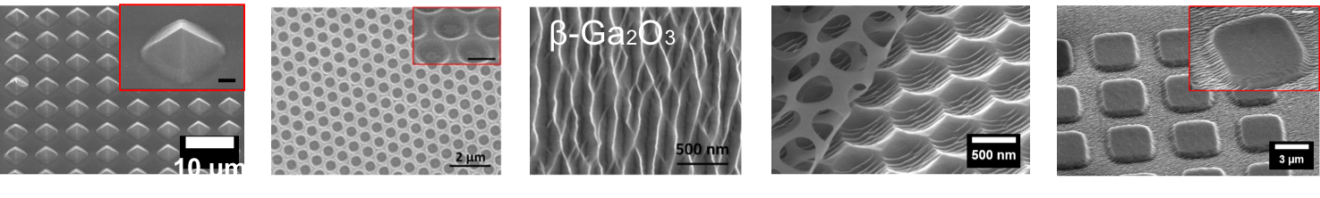
|
Drs. David Ruzic and Jason Peck from the University of Illinois at Urbana-Champaign have developed a new plasma etching process assisted by a polarized pulsed laser. This... Drs. David Ruzic and Jason Peck from the University of Illinois at Urbana-Champaign have developed a new plasma etching process assisted by a polarized pulsed laser. This technology addresses the need of damageless, anisotropic etching for features of 100 nm or less. It is the only known process to etch 3D structures in integrated circuits which lie along one direction, and not etch those that are perpendicular. It will enable making integrated circuits with smaller feature sizes. |
Dr. John Abelson has developed an area selective CVD metal deposition technology. This technology can selectively deposit thin metal layer on a surface. By using... Dr. John Abelson has developed an area selective CVD metal deposition technology. This technology can selectively deposit thin metal layer on a surface. By using inhibitor, one can precisely deposit metal layer only on the position user wants. This technique can save steps in current metal deposition and metal patterning process, thus reducing manufacturing cost. 
|
Dr. Gaurav Bahl from the University of Illinois at Urbana-Champaign has developed a nanophotonic non-reciprocal circuit. The invention allows light to travel only in one... Dr. Gaurav Bahl from the University of Illinois at Urbana-Champaign has developed a nanophotonic non-reciprocal circuit. The invention allows light to travel only in one direction and has great application potential in atomic clocks, gravimetry and optical isolators. This is the first time that any circuit that has been able to operate in the GHz region. |
Dr. Paul Braun from the University of Illinois at Urbana-Champaign has developed a new design architecture for backlit LCDs.... Dr. Paul Braun from the University of Illinois at Urbana-Champaign has developed a new design architecture for backlit LCDs. |
Dr. Seok Kim from the University of Illinois at Urbana-Champaign has developed a versatile surface material that will serve as a general-purpose platform for fluid and... Dr. Seok Kim from the University of Illinois at Urbana-Champaign has developed a versatile surface material that will serve as a general-purpose platform for fluid and light manipulations for micro and macroscale. Potential applications include: digital microfluidics, biomedical devices, virtual blinds, camouflage surfaces, and micromirror arrays. Compared to similar surfaces, this responsive surface consists of micropillars integrated with large area platelets, which increases the areal fraction of opaque regions on the surface and increases the tuning range of transmittance. It does not require heating to create a vapor layer, and allows the use of soft, ferromagnetic micropillars and offers a more efficient assembly process than prior works. Lastly, it allowed control over the final configuration of the platelets, either in-plane or out-of-plane configurations, for the very first time. 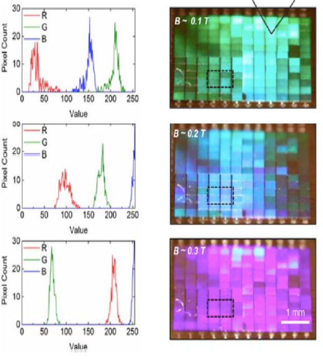
|
This technology enables the fabrication of multiple plans of interconnected passive photonic devices with the volume of a silicon wafer. The fabrication technique uses... This technology enables the fabrication of multiple plans of interconnected passive photonic devices with the volume of a silicon wafer. The fabrication technique uses porous silicon as a scaffold for photoresist in a direct laser write process to make graded index (GRIN) optics and photonic elements. This technology has the potential to dramatically improve the speed, density, and energy efficiency in applications like telecommunications, computing, data storage and transfer and consumer electronics. 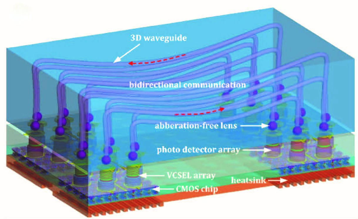
|
Dr. Dragic from the University of IL has developed a low-quantum defect fiber-based laser. This invention assists with the management of... Dr. Dragic from the University of IL has developed a low-quantum defect fiber-based laser. This invention assists with the management of thermal energy (quantum defect heating) which can lead to failure of an optical fiber when power scaling fiber-based lasers. A Yb-doped multicomponent flurosilicate optical fiber reduces quantum defect heating in the fiber-based laser. Fiber-based lasers have applications in the automotive, medical, and electronics industries. 
|
Dr. Songbin Gong and his group from the University of Illinois have developed a framework for synthesizing frequency-independent multi-port nonreciprocal networks. The... Dr. Songbin Gong and his group from the University of Illinois have developed a framework for synthesizing frequency-independent multi-port nonreciprocal networks. The framework is highly expandable, can have an arbitrary number of ports while simultaneously sustaining balanced performance, and provide unprecedented programmability of non-reciprocity. Unlike the conventional approaches, non-reciprocal performance of the network is only dependent of the time delays, instead of phase delays, and therefore is frequency independent. This technology could inspire new ways of implementing multiple input multiple output (MIMO) communication systems. 
4-port switch module prototype |
This technology is a classifier based on a ferroelectric graphene transistor. In contrast to traditional current-mode classifiers based on CMOS technologies (which require... This technology is a classifier based on a ferroelectric graphene transistor. In contrast to traditional current-mode classifiers based on CMOS technologies (which require 23 transistors per pixel), this classifier requires only one transistor per pixel. The device provides a new solution for image recognition with reduced circuit complexity, enhanced energy efficiency, and faster processing speed. Applications include signal or image processing and recognition. |
Dr. Seok Kim and Dr. Moonsub Shim from the University of Illinois have developed dry means to pattern QD films over large areas with high resolution while maintaining... Dr. Seok Kim and Dr. Moonsub Shim from the University of Illinois have developed dry means to pattern QD films over large areas with high resolution while maintaining desired properties. This method avoids standard solution based processing and microfabrication methods which are chemically incompatible with quantum dots. Their method of transfer printing is a scalable and cost-effective approach to manufacturing the next generation of QD lighting, display, and photovoltaic technology. 
Photoluminescence (PL) images of patterned QD films on ODTS coated Si substrates. (a) Red, green, and blue (RGB) QD films patterned in circle, triangle, and star shapes. (b) RGB QD square arrays. (c) Red QD film patterned into ‘UIUC’. All scale bars are 50 microns. (d) PL spectra of patterned RGB QD films. |
Professor Gary Eden from the University of Illinois has developed a device that leverages the recent development of efficient, flat vacuum ultraviolet/ultraviolet lamps to... Professor Gary Eden from the University of Illinois has developed a device that leverages the recent development of efficient, flat vacuum ultraviolet/ultraviolet lamps to perform two or more semiconductor fabrication processes in the same chamber. This invention is expected to significantly lower the cost of manufacturing electronic devices. This invention also introduces a new photolithography process that does not require chemical processing of a photoresist in a separate tool or by wet chemical processing. This process alone will lower the cost of photolithography and make sub-200 nm resolution photolithography accessible to a broader community of users. 
Fig: SEMS of patterns formed in acrylic films by irradiating the films through a photomask with a 172 nm flat lamp |
Dr. Milton Feng, from the University of Illinois, has developed single mode Oxide-VCSELs that are able to transmit data signals over longer distances, at higher speeds... Dr. Milton Feng, from the University of Illinois, has developed single mode Oxide-VCSELs that are able to transmit data signals over longer distances, at higher speeds and with better fidelity than previously possible. Using self-aligned oxidation procedure they are able to uniformly oxidize the mode selective aperture layer and achieve higher transmission rates without sacrificing fidelity. VCSELs are important for use in 3D biosensors, consumer electronics as well as industrial cutting. |
Dr. Dragic from the University of IL has developed a phase and intensity modulator using rare earth doped ytterbium fiber. The modulators are unconventional because they... Dr. Dragic from the University of IL has developed a phase and intensity modulator using rare earth doped ytterbium fiber. The modulators are unconventional because they do not cause phase change through the passage of light. The fiber absorbs the light and heats up causing phase change to occur. |
This portfolio includes carbon nanotube growth and processing methods relevant to nanotube manufacturing.... This portfolio includes carbon nanotube growth and processing methods relevant to nanotube manufacturing. Patterned Catalyst Techniques for Aligned Single-walled Carbon Nanotube GrowthSingle-walled carbon nanotubes (SWNTs) feature exceptional electric properties (conductivity and semi-conductivity) that make them attractive for nano-electronics, optics, material applications and more. This SWNT growth technology yields a dense structure without degraded alignment by eliminating undesired interactions between the SWNT and catalysts on the growth surface. More specifically, a patterned catalyst is used to provide a template to direct SWNT growth, resulting in perfectly aligned high coverage SWNTS. Benefits - Higher density
- Large scale
- Higher quality
Applications - Patterned catalyst techniques are applicable for standard electronic devices that use thin film semiconductors, such as field effect transistors (FETs), sensors, thin-film transistors (TFTs). These devices can benefit from ability to deposit SWNT onto plastics and other unusual device substrates: steerable antenna arrays, flexible displays, etc.
Medium Scale Carbon Nanotube Thin Film Integrated Circuits on Flexible Plastic SubstratesThis technology improves the performance and consistency of integrated circuits featuring semi-conductive carbon nanotube (CNT) transistors. Specifically, metallic conductive pathways in random nanotube networks are reduced using a medium scale carbon nanotube thin film. This process reduces these pathways by cutting fine lines into the carbon nanotube network while preserving its semiconducting properties. Benefits - Reduces purely metallic conductive pathways in a carbon nanotube network used to construct electronic circuits.
- Vastly improves carbon nanotube device consistency in production (yield).
Applications - Primary application is integrated circuits for flexible substrate materials.
Using Nanoscale Thermocapillary Flows to Create Arrays of Purely Semiconducting Single-Walled Carbon NanotubesThis carbon nanotube (CNT) purification technology facilitates scalable, damage-free separation of arrayed metallic and semi-conductive CNTs. Resulting CNT arrays may be large and feature high Ion/Ioff ratios, allowing for less power loss while powered off, faster switching times, and overall lower operating voltage. The invention improves CNT array quality by creating a temperature gradient to release metallic CNTs from the array matrix. Benefits - Less lost power while off
- Faster switching time
- Lower operating voltage
|
Transient electronic devices belong to a set of technologies, whereby traditional analog electronic circuits and components have been made in new ways. These new electronics exist on a much smaller scale and made of bioinert or biocompatible materials. They are flexible and transient. Transient and bioresorbable technologies are a class of device that have the ability to physically disappear at a programmed rate. Inventions within this suite includedevices and processes with applications rangingfrom medicine to construction, and from defense/securityto indoor/outdoor sensors. These technologies are appropriate for applications where device placement can be costly, invasive, or inconvenient to retrieve. Features - Tunable to dissolve at programmed time
 Bio-compatible Bio-compatible- Soft, curvilinear surface
- Transient battery
- Materials: silicon, magnesium, magnesium oxide
Benefits Electronics can now be implanted on surfaces with non-planar contact patches and non-invasive integration on soft, curvilinear surfaces of biological tissues and organs. Application Areas Remaking electronics with these capabilities permits for a plethora of new applications, in medicine, environmental research, biological enhancement, digital financial transactions and traceless surveillance. |
Semiconductor defect detection using Machine Learning Dr. Goddard and Dr. Schwing have developed a machine learning technique which requires only... Semiconductor defect detection using Machine Learning Dr. Goddard and Dr. Schwing have developed a machine learning technique which requires only few training images to detect and classify nano-scale anomalies in semiconductors and in noisy optical images. It is able to automate defect inspection in a 9nm semiconductor wafer with high accuracy and at a high speed in fabrication laboratories using visible light microscopy. This method is faster than atomic force microscopy and scanning electron microscopy, and is more sensitive than current optical microscopy. It can also be used for other applications such as dimension measurements and disease sample measurements. Sanyogita Purandare, Jinlong Zhu, Renjie Zhou, Gabriel Popescu, Alexander Schwing, and Lynford L. Goddard, "Optical inspection of nanoscale structures using a novel machine learning based synthetic image generation algorithm," Opt. Express 27, 17743-17762 (2019) Optical inspection of nanoscale structures using a novel machine learning based synthetic image generation algorithm. Sanyogita Purandare, Jinlong Zhu, Renjie Zhou, Gabriel Popescu, Alexander Schwing, Lynford L. GoddardOpt Express. 2019 Jun 24; 27(13): 17743–17762. doi: 10.1364/OE.27.017743 |
Dr. Eden at the University of Illinois has developed a 3D microplasma photonic crystal which provides the ability to introduce or completely suppress attenuation... Dr. Eden at the University of Illinois has developed a 3D microplasma photonic crystal which provides the ability to introduce or completely suppress attenuation resonances at will, in the microwave, millimeter wave, and terahertz spectral regions, while minimizing insertion loss. This complex 3D photonic crystal is comprised of a 3D-printed polymer scaffold, and free-standing arrays of polyimide capillaries. Since the capillaries are suspended in free space on the scaffold, electromagnetic structures can be placed on or around the microtubes. One example of this involves depositing metal films onto each capillary with precise periodicity. In this way, each pair of neighboring metal film rings in the 3D array are effectively coupled and constitute a capacitor, creating extremely versatile, and tunable crystal performance. Applications Microwave, millimiter-wave, terahertz communications, DoD/military (optical cloaking, electronic warfare) |
Dr. Vasudevan from the University of IL has developed an advanced algorithm for optimizing design-for-debug hardware. This algorithm takes advantage of high level... Dr. Vasudevan from the University of IL has developed an advanced algorithm for optimizing design-for-debug hardware. This algorithm takes advantage of high level abstraction to enable accurate bug localization, eliminating almost 90% of possible root causes in tests using an industrial SoC. This technology, which is broadly scalable versus existing methods, addresses a great need in the field of Electronic Design Automation by decreasing the cost and shortening the timescale of chip debugging, accelerating time-to-market and streamlining the post-silicon validation phase. Application: Incorporation into chip design and verification software Publication: Pal, D.; Sharma, A.; Ray, S.; de Paula, F. M.; and Vasudevan, S. In Proceedings of the 55th Annual Design Automation Conference, DAC 2018, San Francisco, CA, USA, June 24-29, 2018, pages 92:1–92:6, 2018. |
Dr. Yurii Vlasov from the University of Illinois has developed a single-chip neural nanodialysis probe that can sample in vivo brain chemicals, store them, and then... Dr. Yurii Vlasov from the University of Illinois has developed a single-chip neural nanodialysis probe that can sample in vivo brain chemicals, store them, and then directly deploy them for analysis, all while maintaining high temporal resolution. This device uses reversible inlets-outlets and embedded ionization ports to both sample in vivo brain chemicals and deploy them, without need for intermediate storage. This risks less contamination or Taylor dispersion than other methods, and reduces the need for bulky peripherals. ApplicationThis can be used for collecting and analyzing in-vivo biochemical concentrations in the brain. BenefitsThis is a single chip silicon neural probe that can sample live chemicals, store them, and then directly deploy them for analysis. Other neural probes cannot store and deploy these chemical samples, which reduces the temporal resolution of the samples. |
|
Dr. Songbin Gong from the University of Illinois has developed a suite of technologies for the design strategy and method of fabricating acoustic front-end filters at various frequencies,... Dr. Songbin Gong from the University of Illinois has developed a suite of technologies for the design strategy and method of fabricating acoustic front-end filters at various frequencies, including frequencies > 6 GHz. These acoustic front-end filters demonstrate high electromechanical coupling, high fractional bandwidths, as well as high quality factors. This is achieved through a combination of materials selection, resonator design, and filter design. This technology: - Increases the frequency range and the fractional bandwidth of acoustic filters
- Enables the future generations of wireless communication
- Allows access to frequency bands above 6 GHz and provides the high FBW required for 5G communications
 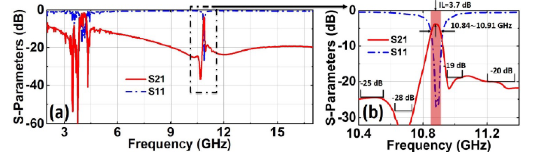
|
This technology leverages the bending stiffness and super lubricity of few-layer materials to create ultra-flexible 2D materials with tunable electronic properties.... This technology leverages the bending stiffness and super lubricity of few-layer materials to create ultra-flexible 2D materials with tunable electronic properties. Applications include MEMS actuators and flexible/stretchable electronics, as well as the miniaturization of a variety of macroscale actuator devices. |
Inventors from the University of Illinois have developed novel phase-separated optical fibers for use in a distributed sensor. These phase-separated optical fibers have... Inventors from the University of Illinois have developed novel phase-separated optical fibers for use in a distributed sensor. These phase-separated optical fibers have high loss (0.05 to 5 dB/m @ 1550 nm) when compared with conventional optical fibers, and the loss dominated by Rayleigh scattering. Moreover, these phase separated fibers are produced through a molten core method (MCM) which makes the cost of production relatively low when compared with conventional fibers. When employed in a Rayleigh based distributed sensor these phase-separated optical fibers provide short-range sensitivity that is orders of magnitude greater than conventional fibers. |
Dr. Alexey Bezryadin, with his research group, has developed a dielectric capacitor that provides 200 J/g of storage density. By injecting and trapping charges within a... Dr. Alexey Bezryadin, with his research group, has developed a dielectric capacitor that provides 200 J/g of storage density. By injecting and trapping charges within a thin dielectric layer, a Coulomb barrier is created that prevents leakage currents that cause capacitors to discharge more quickly. Initial applications for the technology are in cold electronics, which could include quantum computing, space technologies, infrared cameras, or MRI machines. |
This method of forming a nanoscale three-dimensional pattern in a porous semiconductor includes providing a film comprising a semiconductor material and defining a... This method of forming a nanoscale three-dimensional pattern in a porous semiconductor includes providing a film comprising a semiconductor material and defining a nanoscale metal pattern on the film, where the metal pattern has at least one lateral dimension of about 100 nm or less in size. Semiconductor material is removed from below the nanoscale metal pattern to create trenches in the film having a depth-to-width aspect ratio of at least about 10:1, while pores are formed in remaining portions of the film adjacent to the trenches. The method can be extended to form self-integrated porous low-k dielectric insulators with copper interconnects. |
This technology is a new method for creating high aspect ratio III-V semiconductor nanostructures. Unlike currently used commercial technologies, this method does not... This technology is a new method for creating high aspect ratio III-V semiconductor nanostructures. Unlike currently used commercial technologies, this method does not damage the crystal lattice of the existing structure, thus eliminating defects that hinder the material’s transport and optical properties. |
Standard red LEDs suffer from rapid degradation and low efficiency, which becomes increasingly poor at smaller dimensions. Dr. Lee’s novel LED design integrates InP... Standard red LEDs suffer from rapid degradation and low efficiency, which becomes increasingly poor at smaller dimensions. Dr. Lee’s novel LED design integrates InP quantum dots to overcome the deleterious sidewall recombination that reduces the performance of conventional red LEDs. This technology dramatically increases the defect tolerance of red LEDs, with devices showing comparable performance when grown on a range of surfaces including GaAs and GaAs/Si. |
Dr. Seebauer from the University of Illinois has developed a method to eliminate oxygen vacancy defects in thin-film metal oxides. The novel method of a liquid environment... Dr. Seebauer from the University of Illinois has developed a method to eliminate oxygen vacancy defects in thin-film metal oxides. The novel method of a liquid environment enables the improvement of these materials without involving a normally difficult manufacturing process. The process enables the control of oxygen vacancies to a certain depth and density. The removal of the defect allows for the metal oxide thin-film to have better photocatalytic properties. This could be useful for sensors and power devices which are a quickly growing market. The filled vacancies also affect subsequent redox reactions by inhibiting the transfer of electrons.
|
Professor Dallesassee and coworkers from the University of Illinois has developed a method for the heterogeneous integration of III-Nitride materials on various... Professor Dallesassee and coworkers from the University of Illinois has developed a method for the heterogeneous integration of III-Nitride materials on various non-native substrates. This method uses a carrier wafer for the fabrication of the III-Nitride devices, which are then transferred to a host wafer and eutectically bonded. The method takes advantage of current tooling and allows for the fabrication of optoelectronic devices embedded into a CMOS platform for full electronic controls on a common substrate, such as silicon. These technique overcomes many of the limitations currently associated with the integration of III-Nitride materials such as their sub-par thermal performance, and the high costs associated with the handling and alignment of the III-Nitride devices onto the substrate.  
|
Professor Songbin Gong and researchers from the Department of Electrical and Computer Engineering have developed a design strategy and method for fabricating efficient... Professor Songbin Gong and researchers from the Department of Electrical and Computer Engineering have developed a design strategy and method for fabricating efficient piezoelectric micro-machined ultrasonic transducer (pMUT) optimizing both ultrasonic transmitter and receiver performance in a combined platform. Currently, there are two leading material types for pMUTs : ferroelectric perovskites with solid solutions containing PbTiO3, like PZT and PMN-PT (primarily used as transducers ) and the non-ferroelectric structures such as AlN (primarily used as sensors). This balanced ultrasonic transceiver can be implemented in miniature ultrasound applications, specifically in consumer electronics for gesture recognition, biometric sensing and occupancy sensing. |
Researchers from the University of Illinois, along with their collaborators at Eden Park Illumination, have developed a new miniaturized lamp for uses in atomic clocks and... Researchers from the University of Illinois, along with their collaborators at Eden Park Illumination, have developed a new miniaturized lamp for uses in atomic clocks and environmental sensors. These atomic clocks are highly useful in autonomous vehicles due to the precision and accuracy they provide. While most lamps use direct electron impact, this new lamp takes advantage of atomic excitation transfer to increase the efficiency of the lamp. This process reduces the size, and therefore the cost, of producing the lamp. Utilizing smaller lamps will allow for atomic clocks to be more easily integrated into commercial vehicles. Several iterations of the Hg+ lamp have been tested and can be made as small as 0.25 cm3. |
Dr. Rakesh Kumar and his team have developed a new system and tool to analyze logic circuits and find opportunity to automatically optimize them. This technology... Dr. Rakesh Kumar and his team have developed a new system and tool to analyze logic circuits and find opportunity to automatically optimize them. This technology automatically identifies unused instructions from microprocessors that an application is guaranteed not to exercise, eliminates these components and optimizes the design to reduce their cost, area and power requirement. This system uses a combination of techniques that differ from prior methods and leads to improved results. Instead of adding instructions to a specific design, it automatically removed unused ones and generates enhanced hardware from arbitrary designs. |
Researchers at the University of Illinois have developed ultra-flexible heterostructures made from 2D layers of van der Waals bonded materials. The heterostructures retain... Researchers at the University of Illinois have developed ultra-flexible heterostructures made from 2D layers of van der Waals bonded materials. The heterostructures retain the optoelectronic properties of their constituent layers, but offer tunable mechanical properties which can include flexibility rivaling that of lipid bilayers. Applications for this technology include MEMS devices and flexible, stretchable, and conformal circuitry, including reconfigurable 2D devices and folded/curved/crumpled nanostructures. |
Researchers from the University of Illinois have developed a platform for stretchable + flexible optoelectronics that offer consistent performance in stretched vs. non-... Researchers from the University of Illinois have developed a platform for stretchable + flexible optoelectronics that offer consistent performance in stretched vs. non-stretched mode. The platform, which features stacked layers of two-dimensional materials that are crumpled or wrinkled, can enable new designs and manufacturing methodologies for devices that offer both toughness and malleability at scales as small as nanometers. 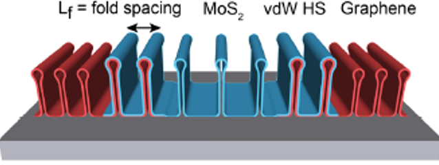 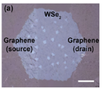 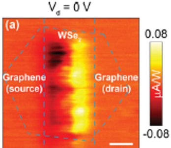
|
Researchers at the University of Illinois have developed a three-dimensional high electron mobility transistor (HEMT) architecture that utilizes ultra-wide bandgap (UWBG)... Researchers at the University of Illinois have developed a three-dimensional high electron mobility transistor (HEMT) architecture that utilizes ultra-wide bandgap (UWBG) materials. These structures and devices can be used for high-power, high-frequency applications, where they can confer an order of magnitude higher performance than wide bandgap (WBG) devices, including simultaneously achieving 10x higher power density while operating at frequencies as high as 120 GHz. |
Capturing polarized and visible light simultaneously is usually achieved by either rotating filters that reduce frame rate and need a static image or using an array of... Capturing polarized and visible light simultaneously is usually achieved by either rotating filters that reduce frame rate and need a static image or using an array of sensors that must be aligned and can be bulkily and expensive. These issues are solved by Dr. Viktor Gruev's invention of a single chip that can detect both kinds of light simultaneously with high resolution and in real time. This sensor can detect 12 bands of visible light and 3 bands of polarized light. Because data is gathered in real time and does not require rotating filters, this sensor has applications in military surveillance, particularly in hazy conditions such as fog or underwater where polarized imaging can reduce background scattering information. Additionally, this sensor can be used in image-guided surgery, such as tumor removal used in combination with injected dyes that bind to cancerous cells that respond to different kinds of light. |
Researchers at the University of Illinois have developed improvements to their innovative photonic integrated circuit (PIC) design, which features three-dimensional... Researchers at the University of Illinois have developed improvements to their innovative photonic integrated circuit (PIC) design, which features three-dimensional subsurface networks of optical components (UIUC ref. no. 2017-212). The paradigm, called "volumetric photonic integrated circuits" (VPIC), addresses the bottleneck of large surface area requirements faced by conventional PICs by embedding the networks vertically within a semiconductor (e.g., porous silicon) material. The present improvements include a variety of new subsurface components which exhibit low loss and high total efficiency competitive with silicon photonics. Components include high Q microrings; lenses and waveguides for efficient coupling; Mach Zehnder interferometers; loop mirrors; and distributed Bragg reflectors. |
University of Illinois Urbana-Champaign researchers Songbin Gong, Ruochen Lu, Yansong Yang, and Steffen Link have fabricated an acoustic filter that functions with high... University of Illinois Urbana-Champaign researchers Songbin Gong, Ruochen Lu, Yansong Yang, and Steffen Link have fabricated an acoustic filter that functions with high fractional bandwidth and low signal loss at gigahertz frequencies necessary for emerging 5G new radio technologies. The acoustic filter is suitable for 5G mobile devices (e.g. smart phones), which will employ wavebands of higher frequencies than 4G technology. The device maintains small proportions without the fabrication challenges seen from scaling existing acoustic filter components present in 4G devices. The filter employs a double layer of thin-film lithium niobate, a piezoelectric material, which serves to convert mechanical energy (radio waves) to electronic signals in 5G devices with better performance in the 3-6 GHz range than existing technologies. |