

This portfolio includes carbon nanotube growth and processing methods relevant to nanotube manufacturing.
Patterned Catalyst Techniques for Aligned Single-walled Carbon Nanotube Growth
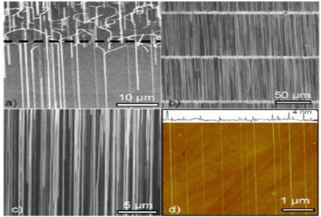
Single-walled carbon nanotubes (SWNTs) feature exceptional electric properties (conductivity and semi-conductivity) that make them attractive for nano-electronics, optics, material applications and more. This SWNT growth technology yields a dense structure without degraded alignment by eliminating undesired interactions between the SWNT and catalysts on the growth surface. More specifically, a patterned catalyst is used to provide a template to direct SWNT growth, resulting in perfectly aligned high coverage SWNTS.
Benefits
- Higher density
- Large scale
- Higher quality
Applications
- Patterned catalyst techniques are applicable for standard electronic devices that use thin film semiconductors, such as field effect transistors (FETs), sensors, thin-film transistors (TFTs). These devices can benefit from ability to deposit SWNT onto plastics and other unusual device substrates: steerable antenna arrays, flexible displays, etc.
Medium Scale Carbon Nanotube Thin Film Integrated Circuits on Flexible Plastic Substrates
This technology improves the performance and consistency of integrated circuits featuring semi-conductive carbon nanotube (CNT) transistors. Specifically, metallic conductive pathways in random nanotube networks are reduced using a medium scale carbon nanotube thin film. This process reduces these pathways by cutting fine lines into the carbon nanotube network while preserving its semiconducting properties.
Benefits
- Reduces purely metallic conductive pathways in a carbon nanotube network used to construct electronic circuits.
- Vastly improves carbon nanotube device consistency in production (yield).
Applications
- Primary application is integrated circuits for flexible substrate materials.
Using Nanoscale Thermocapillary Flows to Create Arrays of Purely Semiconducting Single-Walled Carbon Nanotubes
This carbon nanotube (CNT) purification technology facilitates scalable, damage-free separation of arrayed metallic and semi-conductive CNTs. Resulting CNT arrays may be large and feature high Ion/Ioff ratios, allowing for less power loss while powered off, faster switching times, and overall lower operating voltage. The invention improves CNT array quality by creating a temperature gradient to release metallic CNTs from the array matrix.
Benefits
- Less lost power while off
- Faster switching time
- Lower operating voltage