

Professor Gary Eden from the University of Illinois has developed a device that leverages the recent development of efficient, flat vacuum ultraviolet/ultraviolet lamps to perform two or more semiconductor fabrication processes in the same chamber. This invention is expected to significantly lower the cost of manufacturing electronic devices. This invention also introduces a new photolithography process that does not require chemical processing of a photoresist in a separate tool or by wet chemical processing. This process alone will lower the cost of photolithography and make sub-200 nm resolution photolithography accessible to a broader community of users.
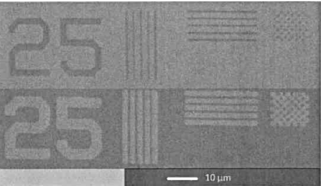
Fig: SEMS of patterns formed in acrylic films by irradiating the films through a photomask with a 172 nm flat lamp