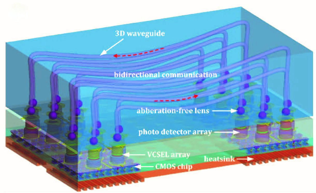
This technology enables the fabrication of multiple plans of interconnected passive photonic devices with the volume of a silicon wafer. The fabrication technique uses porous silicon as a scaffold for photoresist in a direct laser write process to make graded index (GRIN) optics and photonic elements. This technology has the potential to dramatically improve the speed, density, and energy efficiency in applications like telecommunications, computing, data storage and transfer and consumer electronics.


